- 您现在的位置:买卖IC网 > PDF目录10735 > ADCMP572BCPZ-WP (Analog Devices Inc)IC COMPARATOR CML 3.3-5V 16LFCSP PDF资料下载
参数资料
| 型号: | ADCMP572BCPZ-WP |
| 厂商: | Analog Devices Inc |
| 文件页数: | 2/16页 |
| 文件大小: | 0K |
| 描述: | IC COMPARATOR CML 3.3-5V 16LFCSP |
| 标准包装: | 50 |
| 类型: | 带锁销 |
| 元件数: | 1 |
| 输出类型: | CML,补充型 |
| 电压 - 电源,单路/双路(±): | 3.1 V ~ 5.4 V |
| 电压 - 输入偏移(最小值): | 2mV @ 3.3V |
| 电流 - 输入偏压(最小值): | 25µA @ 3.3V |
| 电流 - 输出(标准): | 20mA |
| 电流 - 静态(最大值): | 52mA |
| CMRR, PSRR(标准): | 65dB CMRR,74dB PSRR |
| 传输延迟(最大): | 0.165ns |
| 磁滞: | ±1mV |
| 工作温度: | -40°C ~ 85°C |
| 封装/外壳: | 16-VFQFN 裸露焊盘,CSP |
| 安装类型: | 表面贴装 |
| 包装: | 托盘 - 晶粒 |
| 配用: | EVAL-ADCMP572BCPZ-ND - BOARD EVALUATION ADCMP572BCP |
ADCMP572/ADCMP573
Rev. A | Page 10 of 16
500 Ω resistor and leaving the LE pin disconnected. In this case,
the resistor value does not depend on the VCCO supply voltage.
VCCO is the signal return for the output stage and VCCO pins
should of course be connected to a supply plane for maximum
performance.
OPTIMIZING HIGH SPEED PERFORMANCE
As with any high speed comparator, proper design and layout
techniques are essential to obtaining the specified performance.
Stray capacitance, inductance, inductive power and ground
impedances, or other layout issues can severely limit
performance and often cause oscillation. Discontinuities along
input and output transmission lines can severely limit the
specified pulse width dispersion performance.
For applications working in a 50 Ω environment, input and
output matching has a significant impact on data dependent (or
deterministic) jitter (DJ) and on pulse width dispersion
performance. The ADCMP572/ADCMP573 comparators
provide internal 50 Ω termination resistors for both the VP and
VN inputs, and the ADCMP572 provides 50 Ω back terminated
outputs. The return side for each input termination is pinned
out separately with the VTP and VTN pins, respectively. If a 50 Ω
termination is desired at one or both of the VP/VN inputs, then
the VTP and VTN pins can be connected (or disconnected) to
(from) the desired termination potential as required. The
termination potential should be carefully bypassed using high
quality bypass capacitors as discussed earlier to prevent
undesired aberrations on the input signal due to parasitic
inductance in the circuit board layout. If a 50 Ω input
termination is not desired, either one or both of the VTP/VTN
termination pins can be left disconnected. In this case, the pins
should be left floating with no external pull-downs or bypassing
capacitors.
When leaving an input termination disconnected, the internal
resistor acts as a small stub on the input transmission path and
can cause problems for very high speed inputs. Reflections
should then be expected from the comparator inputs because
they no longer provide matched impedance to the input path
leading to the device. In this case, it is important to back match
the drive source impedance to the input transmission path to
minimize multiple reflections. For applications in which the
comparator is very close to the driving signal source, the source
impedance should be minimized. High source impedance in
combination with parasitic input capacitance of the comparator
might cause an undesirable degradation in bandwidth at the
input, therefore degrading the overall response. Although the
ADCMP572/ADCMP573 comparators have been designed to
minimize input capacitance, some parasitic capacitance is
inevitable. It is therefore recommended that the drive source
impedance be no more than 50 Ω for best high speed
performance.
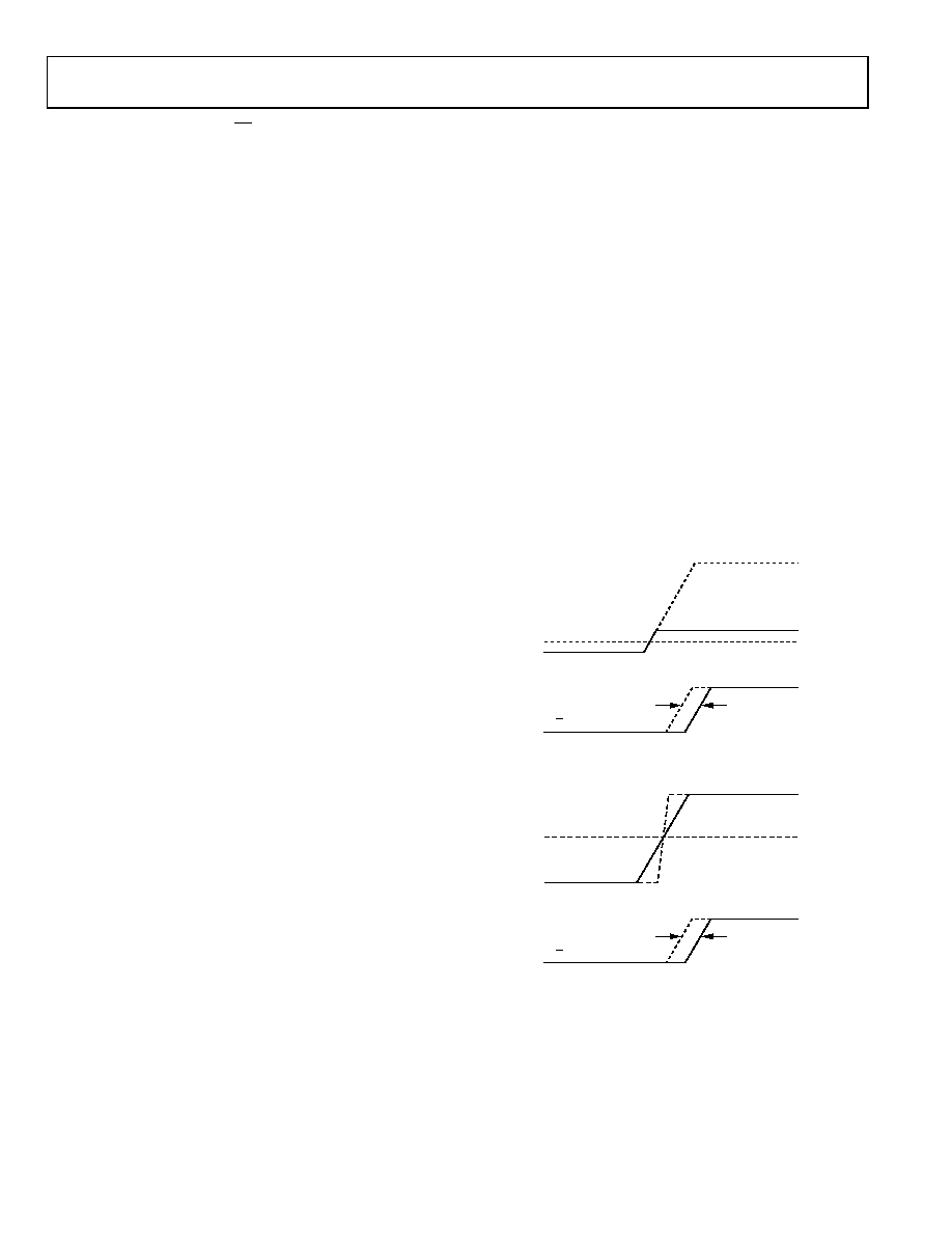
COMPARATOR PROPAGATION
DELAY DISPERSION
The ADCMP572/ADCMP573 comparators are designed to
reduce propagation delay dispersion over a wide input overdrive
range of 5 mV to 500 mV. Propagation delay dispersion is
variation in the propagation delay that results from a change in
the degree of overdrive or slew rate (how far or how fast the
input signal exceeds the switching threshold).
Propagation delay dispersion is a specification that becomes
important in high speed, time-critical applications such as data
communication, automatic test and measurement, instrumenta-
tion, and event driven applications such as pulse spectroscopy,
nuclear instrumentation, and medical imaging. Dispersion is
defined as the variation in propagation delay as the input over-
drive conditions vary (Figure 17 and Figure 18). For the
ADCMP572/ADCMP573, dispersion is typically <15 ps
because the overdrive varies from 10 mV to 500 mV, and the
input slew rate varies from 2 V/ns to 10 V/ns. This specification
applies for both positive and negative signals since the
ADCMP572/ADCMP573 has substantially equal delays for
either positive going or negative going inputs.
Q/Q OUTPUT
INPUT VOLTAGE
500mV OVERDRIVE
10mV OVERDRIVE
DISPERSION
VN ± VOS
04409-0-027
Figure 17. Propagation Delay—Overdrive Dispersion
Q/Q OUTPUT
INPUT VOLTAGE
10V/ns
1V/ns
DISPERSION
VN ± VOS
04409-0-028
Figure 18. Propagation Delay—Slew Rate Dispersion
相关PDF资料 |
PDF描述 |
|---|---|
| VE-J4V-MY-F4 | CONVERTER MOD DC/DC 5.8V 50W |
| VI-JNW-MY-F2 | CONVERTER MOD DC/DC 5.5V 50W |
| VE-2WN-MY-B1 | CONVERTER MOD DC/DC 18.5V 50W |
| VE-2N4-CV-B1 | CONVERTER MOD DC/DC 48V 150W |
| VE-2WM-MY-B1 | CONVERTER MOD DC/DC 10V 50W |
相关代理商/技术参数 |
参数描述 |
|---|---|
| ADCMP572XCP | 制造商:Analog Devices 功能描述:CML ULTRAFAST 3.3V SINGLE SUPPLY COMPARATOR - Bulk |
| ADCMP573 | 制造商:AD 制造商全称:Analog Devices 功能描述:Ultrafast 3.3 V Single-Supply Comparators |
| ADCMP573BCP | 制造商:Analog Devices 功能描述:COMPARATOR SGL 5.4V 16LFCSP EP - Bulk |
| ADCMP573BCP-R2 | 制造商:Rochester Electronics LLC 功能描述: 制造商:Analog Devices 功能描述: |
| ADCMP573BCPRL7 | 制造商:AD 功能描述:NEW |
发布紧急采购,3分钟左右您将得到回复。