- 您现在的位置:买卖IC网 > PDF目录10735 > ADCMP572BCPZ-WP (Analog Devices Inc)IC COMPARATOR CML 3.3-5V 16LFCSP PDF资料下载
参数资料
| 型号: | ADCMP572BCPZ-WP |
| 厂商: | Analog Devices Inc |
| 文件页数: | 5/16页 |
| 文件大小: | 0K |
| 描述: | IC COMPARATOR CML 3.3-5V 16LFCSP |
| 标准包装: | 50 |
| 类型: | 带锁销 |
| 元件数: | 1 |
| 输出类型: | CML,补充型 |
| 电压 - 电源,单路/双路(±): | 3.1 V ~ 5.4 V |
| 电压 - 输入偏移(最小值): | 2mV @ 3.3V |
| 电流 - 输入偏压(最小值): | 25µA @ 3.3V |
| 电流 - 输出(标准): | 20mA |
| 电流 - 静态(最大值): | 52mA |
| CMRR, PSRR(标准): | 65dB CMRR,74dB PSRR |
| 传输延迟(最大): | 0.165ns |
| 磁滞: | ±1mV |
| 工作温度: | -40°C ~ 85°C |
| 封装/外壳: | 16-VFQFN 裸露焊盘,CSP |
| 安装类型: | 表面贴装 |
| 包装: | 托盘 - 晶粒 |
| 配用: | EVAL-ADCMP572BCPZ-ND - BOARD EVALUATION ADCMP572BCP |
ADCMP572/ADCMP573
Rev. A | Page 13 of 16
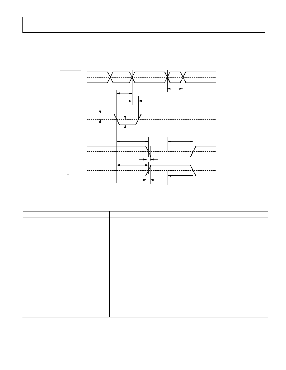
TIMING INFORMATION
Figure 29 illustrates the ADCMP572/ADCMP573 compare and latch timing relationships. Table 4 provides definitions of the terms
shown in the figure.
50%
VN ± VOS
50%
DIFFERENTIAL
INPUT VOLTAGE
LATCH ENABLE
Q OUTPUT
LATCH ENABLE
tH
tPDL
tPDH
tPLOH
tPLOL
tR
tF
VIN
VOD
tS
tPL
04409-003
Figure 29. System Timing Diagram
Table 4. Timing Descriptions
Symbol
Timing
Description
tPDH
Input to output high delay
Propagation delay measured from the time the input signal crosses the reference (± the
input offset voltage) to the 50% point of an output low-to-high transition.
tPDL
Input to output low delay
Propagation delay measured from the time the input signal crosses the reference (± the
input offset voltage) to the 50% point of an output high-to-low transition.
tPLOH
Latch enable to output high delay
Propagation delay measured from the 50% point of the latch enable signal low-to-high
transition to the 50% point of an output low-to-high transition.
tPLOL
Latch enable to output low delay
Propagation delay measured from the 50% point of the latch enable signal low-to-high
transition to the 50% point of an output high-to-low transition.
tH
Minimum hold time
Minimum time after the negative transition of the latch enable signal that the input
signal must remain unchanged to be acquired and held at the outputs.
tPL
Minimum latch enable pulse width
Minimum time that the latch enable signal must be high to acquire an input signal
change.
tS
Minimum setup time
Minimum time before the negative transition of the latch enable signal that an input
signal change must be present to be acquired and held at the outputs.
tR
Output rise time
Amount of time required to transition from a low to a high output as measured at the
20% and 80% points.
tF
Output fall time
Amount of time required to transition from a high to a low output as measured at the
20% and 80% points.
VOD
Voltage overdrive
Difference between the input voltages VA and VB.
相关PDF资料 |
PDF描述 |
|---|---|
| VE-J4V-MY-F4 | CONVERTER MOD DC/DC 5.8V 50W |
| VI-JNW-MY-F2 | CONVERTER MOD DC/DC 5.5V 50W |
| VE-2WN-MY-B1 | CONVERTER MOD DC/DC 18.5V 50W |
| VE-2N4-CV-B1 | CONVERTER MOD DC/DC 48V 150W |
| VE-2WM-MY-B1 | CONVERTER MOD DC/DC 10V 50W |
相关代理商/技术参数 |
参数描述 |
|---|---|
| ADCMP572XCP | 制造商:Analog Devices 功能描述:CML ULTRAFAST 3.3V SINGLE SUPPLY COMPARATOR - Bulk |
| ADCMP573 | 制造商:AD 制造商全称:Analog Devices 功能描述:Ultrafast 3.3 V Single-Supply Comparators |
| ADCMP573BCP | 制造商:Analog Devices 功能描述:COMPARATOR SGL 5.4V 16LFCSP EP - Bulk |
| ADCMP573BCP-R2 | 制造商:Rochester Electronics LLC 功能描述: 制造商:Analog Devices 功能描述: |
| ADCMP573BCPRL7 | 制造商:AD 功能描述:NEW |
发布紧急采购,3分钟左右您将得到回复。