- 您现在的位置:买卖IC网 > PDF目录20638 > ADE7754ARZ (Analog Devices Inc)IC ENERGY METERING 3PHASE 24SOIC PDF资料下载
参数资料
| 型号: | ADE7754ARZ |
| 厂商: | Analog Devices Inc |
| 文件页数: | 10/44页 |
| 文件大小: | 0K |
| 描述: | IC ENERGY METERING 3PHASE 24SOIC |
| 标准包装: | 31 |
| 输入阻抗: | 370 千欧 |
| 测量误差: | 0.1% |
| 电压 - 高输入/输出: | 2.4V |
| 电压 - 低输入/输出: | 0.8V |
| 电流 - 电源: | 7mA |
| 电源电压: | 4.75 V ~ 5.25 V |
| 测量仪表类型: | 3 相 |
| 工作温度: | -40°C ~ 85°C |
| 安装类型: | 表面贴装 |
| 封装/外壳: | 24-SOIC(0.295",7.50mm 宽) |
| 供应商设备封装: | 24-SOIC W |
| 包装: | 管件 |
| 产品目录页面: | 797 (CN2011-ZH PDF) |
| 配用: | EVAL-ADE7754EBZ-ND - BOARD EVALAUTION FOR ADE7754 |
第1页第2页第3页第4页第5页第6页第7页第8页第9页当前第10页第11页第12页第13页第14页第15页第16页第17页第18页第19页第20页第21页第22页第23页第24页第25页第26页第27页第28页第29页第30页第31页第32页第33页第34页第35页第36页第37页第38页第39页第40页第41页第42页第43页第44页
�� ��
��
��ADE7754�
�Figure� 6� shows� how� the� gain� settings� in� PGA� 1� (current� channel)�
�and� PGA� 2� (voltage� channel)� are� selected� by� various� bits� in� the�
�gain� register.� The� no-load� threshold� and� sum� of� the� absolute�
�value� can� also� be� selected� in� the� gain� register.� See� Table� X.�
�GAIN� REGISTER� *�
�CURRENT� AND� VOLTAGE� CHANNEL� PGA� CONTROL�
�spreads� the� quantization� noise� (noise� due� to� sampling)� over� a�
�wider� bandwidth.� With� the� noise� spread� more� thinly� over� a�
�wider� bandwidth,� the� quantization� noise� in� the� band� of� interest�
�is� lowered.� See� Figure� 8.�
�Oversampling� alone� is� not� an� efficient� enough� method� to�
�improve� the� signal� to� noise� ratio� (SNR)� in� the� band� of� interest.�
�7�
�0�
�6�
�0�
�5�
�0�
�4�
�0�
�3�
�0�
�2�
�0�
�1�
�0�
�0�
�0�
�ADDR:� 18h�
�For� example,� an� oversampling� ratio� of� 4� is� required� to� increase�
�the� SNR� by� only� 6� dB� (1� bit).� To� keep� the� oversampling� ratio� at�
�a� reasonable� level,� the� quantization� noise� can� be� shaped� so� that�
�RESERVED� =� 0� RESERVED� =� 0�
�ABS�
�most� of� the� noise� lies� at� the� higher� frequencies.� In� the� Σ� -� ?�
�modulator,� the� noise� is� shaped� by� the� integrator,� which� has� a�
�PGA� 2� GAIN� SELECT�
�00� =� 1�
�NO� LOAD�
�PGA� 1� GAIN� SELECT�
�00� =� 1�
�high-pass� type� of� response� for� the� quantization� noise.� The� result�
�is� that� most� of� the� noise� is� at� the� higher� frequencies,� where� it�
�01� =�
�10� =�
�2�
�4�
�01� =�
�10� =�
�2�
�4�
�can� be� removed� by� the� digital� low-pass� filter.� This� noise� shaping�
�*� REGISTER� CONTENTS� SHOW� POWER-ON� DEFAULTS�
�Figure� 6.� Analog� Gain� Register�
�is� shown� in� Figure� 8.�
�ANTIALIAS� FILTER� (RC)�
�ANALOG-TO-DIGITAL� CONVERSION�
�SIGNAL�
�DIGITAL� FILTER�
�SHAPED�
�NOISE�
�SAMPLING�
�FREQUENCY�
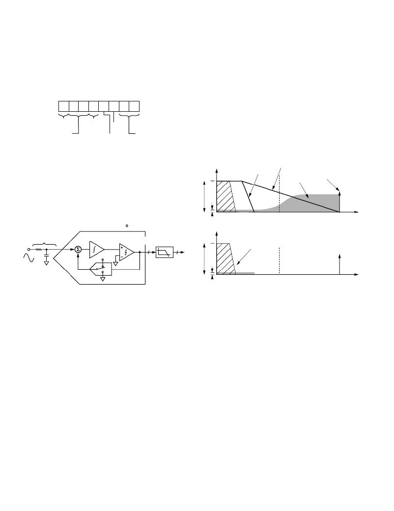
�The� ADE7754� carries� out� analog-to-digital� conversion� using�
�second� order� Σ� -� ?� ADCs.� The� block� diagram� in� Figure� 7� shows� a�
�first� order� (for� simplicity)� Σ� -� ?� ADC.� The� converter� is� made� up� of�
�two� parts,� the� Σ� -� ?� modulator� and� the� digital� low-pass� filter.�
�NOISE�
�MCLK/12�
�0�
�2�
�417�
�FREQUENCY� (kHz)�
�833�
�ANALOG�
�LOW-PASS� FILTER�
�+�
�INTEGRATOR�
�LATCHED�
�COMPARATOR�
�SIGNAL�
�HIGH� RESOLUTION�
�OUTPUT� FROM� DIGITAL�
�R�
�C�
�–�
�V� REF�
�1�
�24�
�LPF�
�DIGITAL�
�LOW-PASS�
�NOISE�
�....10100101......�
�FILTER�
�1-BIT� DAC�
�0�
�2�
�417�
�833�
�Figure� 7.� First� Order� (� -� )� ADC�
�A� Σ� -� ?� modulator� converts� the� input� signal� into� a� continuous�
�serial� stream� of� 1s� and� 0s� at� a� rate� determined� by� the� sampling�
�clock.� In� the� ADE7754,� the� sampling� clock� is� equal� to� CLKIN/12.�
�The� 1-bit� DAC� in� the� feedback� loop� is� driven� by� the� serial� data�
�stream.� The� DAC� output� is� subtracted� from� the� input� signal.�
�If� the� loop� gain� is� high� enough,� the� average� value� of� the� DAC�
�output� (and� therefore� the� bit� stream)� will� approach� that� of� the�
�input� signal� level.� For� any� given� input� value� in� a� single� sampling�
�interval,� the� data� from� the� 1-bit� ADC� is� virtually� meaningless.� Only�
�when� a� large� number� of� samples� are� averaged� will� a� meaningful�
�result� be� obtained.� This� averaging� is� carried� out� in� the� second� part�
�of� the� ADC,� the� digital� low-pass� filter.� Averaging� a� large� number� of�
�bits� from� the� modulator,� the� low-pass� filter� can� produce� 24-bit�
�data-words� that� are� proportional� to� the� input� signal� level.�
�The� Σ� -� ?� converter� uses� two� techniques� to� achieve� high� resolu-�
�tion� from� what� is� essentially� a� 1-bit� conversion� technique.� The�
�first� is� oversampling;� the� signal� is� sampled� at� a� rate� (frequency)�
�many� times� higher� than� the� bandwidth� of� interest.� For� example,�
�the� sampling� rate� in� the� ADE7754� is� CLKIN/12� (833� kHz),�
�and� the� band� of� interest� is� 40� Hz� to� 2� kHz.� Oversampling�
�FREQUENCY� (kHz)�
�Figure� 8.� Noise� Reduction� Due� to� Oversampling�
�and� Noise� Shaping� in� the� Analog� Modulator�
�Antialias� Filter�
�Figure� 7� shows� an� analog� low-pass� filter� (RC)� on� the� input� to�
�the� modulator.� This� filter� is� used� to� prevent� aliasing,� an� artifact�
�of� all� sampled� systems.� Frequency� components� in� the� input�
�signal� to� the� ADC� that� are� higher� than� half� the� sampling� rate� of�
�the� ADC� appear� in� the� sampled� signal� at� a� frequency� below� half�
�the� sampling� rate.� Figure� 9� illustrates� the� effect;� frequency� com-�
�ponents� (arrows� shown� in� black)� above� half� the� sampling�
�frequency� (also� known� as� the� Nyquist� frequency),� i.e.,� 417� kHz,�
�get� imaged� or� folded� back� down� below� 417� kHz� (arrows� shown�
�in� gray).� This� happens� with� all� ADCs,� regardless� of� the� archi-�
�tecture.� In� the� example� shown,� only� frequencies� near� the� sampling�
�frequency,� i.e.,� 833� kHz,� will� move� into� the� band� of� interest� for�
�metering,� i.e.,� 40� Hz� to� 2� kHz.� This� allows� use� of� a� very� simple�
�LPF� (low-pass� filter)� to� attenuate� these� high� frequencies� (near�
�900� kHz)� and� thus� prevent� distortion� in� the� band� of� interest.� A�
�simple� RC� filter� (single� pole)� with� a� corner� frequency� of� 10� kHz�
�produces� an� attenuation� of� approximately� 40� dBs� at� 833� kHz.�
�See� Figure� 9.� This� is� sufficient� to� eliminate� the� effects� of� aliasing.�
�–10� –�
�REV.� 0�
�相关PDF资料 |
PDF描述 |
|---|---|
| MAX8631YETI+ | IC LED DRVR WHITE BCKLGT 28-TQFN |
| EBC15DCMI-S288 | CONN EDGECARD 30POS .100 EXTEND |
| ISL6605IRZ-T | IC MOSFET DRVR SYNC BUCK 8-QFN |
| VI-J6F-CX-F1 | CONVERTER MOD DC/DC 72V 75W |
| PX3511BDAG-R3 | IC DRVR SYNC BUCK HF 8-SOIC |
相关代理商/技术参数 |
参数描述 |
|---|---|
| ADE7754ARZRL | 功能描述:IC ENERGY METERING 3PHASE 24SOIC RoHS:是 类别:集成电路 (IC) >> PMIC - 能量测量 系列:- 产品培训模块:Lead (SnPb) Finish for COTS Obsolescence Mitigation Program 标准包装:2,500 系列:* |
| ADE7755 | 制造商:AD 制造商全称:Analog Devices 功能描述:Energy Metering IC with Pulse Output |
| ADE7755AARSRL | 制造商:Analog Devices 功能描述:ENERGY METERING IC WITH P - Tape and Reel |
| ADE7755AN | 制造商:Rochester Electronics LLC 功能描述: 制造商:Analog Devices 功能描述: |
| ADE7755AN-REF | 制造商:AD 制造商全称:Analog Devices 功能描述:Energy Metering IC with Pulse Output |
发布紧急采购,3分钟左右您将得到回复。