- 您现在的位置:买卖IC网 > PDF目录20638 > ADE7754ARZ (Analog Devices Inc)IC ENERGY METERING 3PHASE 24SOIC PDF资料下载
参数资料
| 型号: | ADE7754ARZ |
| 厂商: | Analog Devices Inc |
| 文件页数: | 16/44页 |
| 文件大小: | 0K |
| 描述: | IC ENERGY METERING 3PHASE 24SOIC |
| 标准包装: | 31 |
| 输入阻抗: | 370 千欧 |
| 测量误差: | 0.1% |
| 电压 - 高输入/输出: | 2.4V |
| 电压 - 低输入/输出: | 0.8V |
| 电流 - 电源: | 7mA |
| 电源电压: | 4.75 V ~ 5.25 V |
| 测量仪表类型: | 3 相 |
| 工作温度: | -40°C ~ 85°C |
| 安装类型: | 表面贴装 |
| 封装/外壳: | 24-SOIC(0.295",7.50mm 宽) |
| 供应商设备封装: | 24-SOIC W |
| 包装: | 管件 |
| 产品目录页面: | 797 (CN2011-ZH PDF) |
| 配用: | EVAL-ADE7754EBZ-ND - BOARD EVALAUTION FOR ADE7754 |
第1页第2页第3页第4页第5页第6页第7页第8页第9页第10页第11页第12页第13页第14页第15页当前第16页第17页第18页第19页第20页第21页第22页第23页第24页第25页第26页第27页第28页第29页第30页第31页第32页第33页第34页第35页第36页第37页第38页第39页第40页第41页第42页第43页第44页
�� �
�
�ADE7754�
�pattern.� Current� rms� measurements� of� Phase� A� are� corrupted� by�
�the� signal� on� the� Phase� C� current� input,� current� rms� measure-�
�ments� of� Phase� B� are� corrupted� by� the� signal� on� the� Phase� A�
�current� input,� and� current� rms� measurements� of� Phase� C� are�
�corrupted� by� the� signal� on� the� Phase� B� current� input.� This�
�crosstalk� is� present� only� on� the� current� rms� measurements� and�
�does� not� affect� the� regular� active� power� measurements.� The�
�level� of� the� crosstalk� is� dependent� on� the� level� of� the� noise�
�source� and� the� phase� angle� between� the� noise� source� and� the�
�corrupted� signal.� The� level� of� the� crosstalk� can� be� reduced� by�
�writing� 01F7h� to� the� address� 3Dh.� This� 16-bit� register� is�
�reserved� for� factory� operation� and� should� not� be� written� to� any�
�other� value.� When� the� current� inputs� are� 120� °� out� of� phase� and�
�the� register� 3Dh� is� set� to� 01F7h,� the� level� of� the� current� rms�
�crosstalk� is� below� 2%.�
�Current� RMS� Gain� Adjust�
�The� active� power� gain� registers� (AAPGAIN[11:0],� BAPGAIN,�
�and� CAPGAIN)� affect� the� active� power� and� current� rms� values.�
�Calibrating� the� current� rms� measurements� with� these� registers� is�
�not� recommended.� The� conversion� of� the� current� rms� registers�
�values� to� amperes� has� to� be� done� in� an� external� microcontroller�
�with� a� specific� ampere/LSB� constant� for� each� phase.� See� the� Cali-�
�bration� of� a� 3-Phase� Meter� Based� on� the� ADE7754� Application�
�Note� AN-624.� Due� to� gain� mismatches� between� phases,� the� cali-�
�bration� of� the� ampere/LSB� constant� has� to� be� done� separately� for�
�each� phase.� One-point� calibration� is� sufficient� for� this� calibration.�
�done� close� to� full� scale� and� the� other� at� approximately� full� scale/�
�100.� The� current� offset� compensation� can� then� be� derived� using�
�these� measurements.� See� the� Calibration� of� a� 3-Phase� Meter� Based�
�on� the� ADE7754� Application� Note� AN-624.�
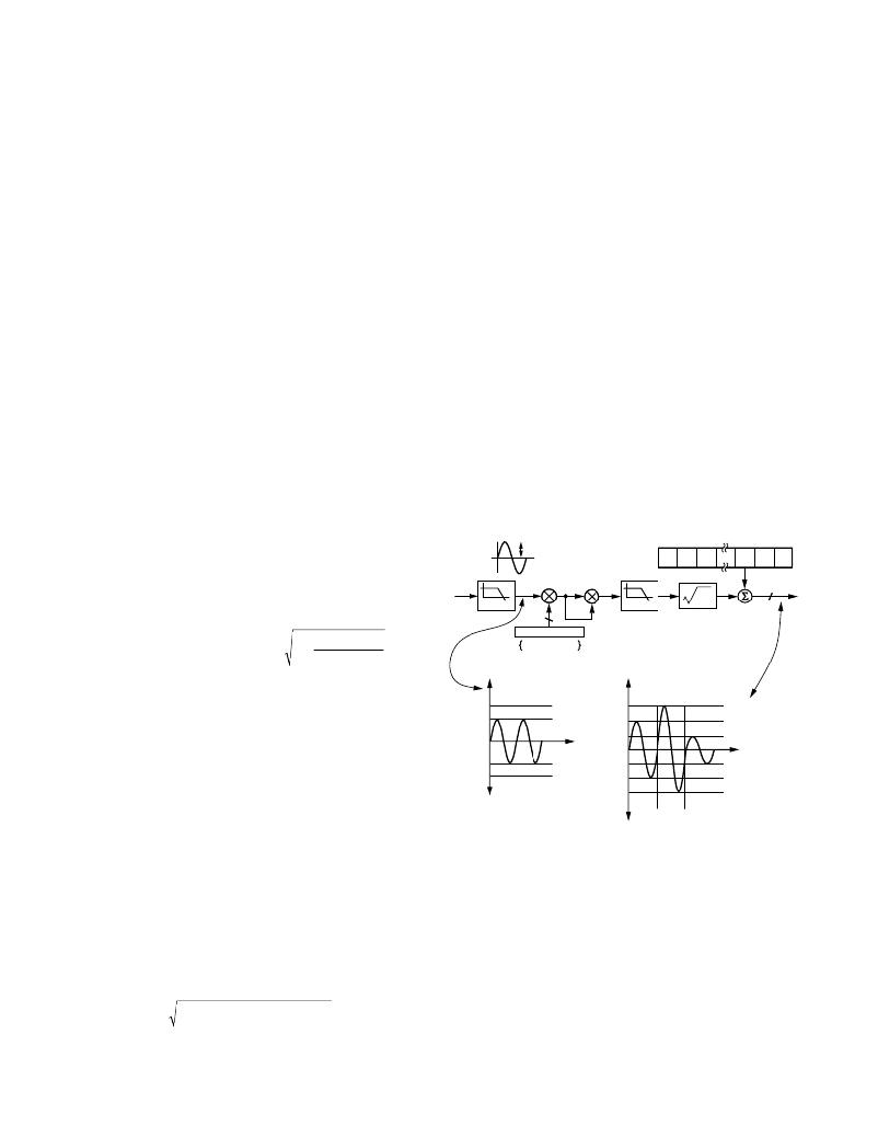
�Voltage� RMS� Calculation�
�Figure� 21� shows� the� details� of� the� signal� processing� chain� for� the�
�rms� calculation� on� one� of� the� phases� of� the� voltage� channel.� The�
�voltage� channel� rms� value� is� processed� from� the� samples� used� in�
�the� voltage� channel� waveform� sampling� mode.� The� output� of�
�the� voltage� channel� ADC� can� be� scaled� by� ±� 50%� by� changing�
�VGAIN� registers� to� perform� an� overall� apparent� power� calibra-�
�tion.� See� the� Apparent� Power� Calculation� section.� The� VGAIN�
�adjustment� affects� the� rms� calculation� because� it� is� done� before�
�the� rms� signal� processing.� The� voltage� rms� values� are� stored� in�
�unsigned� 24-bit� registers� (AVRMS,� BVRMS,� and� CVRMS).�
�256� LSB� of� the� voltage� rms� register� is� approximately� equivalent�
�to� one� LSB� of� a� voltage� waveform� sample.� The� update� rate� of�
�the� voltage� rms� measurement� is� CLKIN/12.�
�With� the� specified� full-scale� ac� analog� input� signal� of� 0.5� V,� the�
�LPF1� produces� an� output� code� that� is� approximately� ±� 10,217�
�decimal� at� 60� Hz.� See� the� Voltage� Channel� ADC� section.� The�
�equivalent� rms� value� of� a� full-scale� ac� signal� is� approximately�
�7,221d� (1C35h),� which� gives� a� voltage� rms� value� of� 1,848,772d�
�(1C35C4h)� in� the� V� RMS� register.� With� offset� calibration,� the�
�voltage� rms� measurement� provided� in� the� ADE7754� is� accurate�
�within� ±� 0.5%� for� signal� input� between� full� scale� and� full� scale/20.�
�The� active� power� gain� registers� ease� the� calibration� of� the� active�
�energy� calculation� in� MODE� 1� and� 2� of� the� WATMODE� register.�
�VOLTAGE� SIGNAL� –� V(t)�
�0.5/GAIN2�
�VRMSOS[11:0]�
�Current� rms� register� Phase� A� =� ?� rms� � 1� +�
�?�
�?�
�If� the� APGAIN� registers� are� used� for� active� power� calibration�
�(WATMOD� bits� in� WATMode� register� =� 1� or� 2),� the� current�
�rms� values� are� changed� by� the� active� power� gain� register� value�
�as� described� in� the� expression�
�?�
�AAPGAIN� ?�
�2� 12�
�?�
�VA�
�LPF1�
�VOLTAGE�
�SIGNAL� –� v(t)�
�12�
�800h–7FFh�
�AVGAIN[11:0]�
�LPF3�
�VOLTAGE�
�CHANNEL� (rms)�
�SGN� 2� 11�
�2� 8�
�+�
�2� 2�
�+�
�2� 1�
�24�
�2� 0�
�For� example,� when� 7FFh� is� written� to� the� active� power� gain�
�register,� the� ADC� output� is� scaled� up� by� 22.5%.� Similarly,� 800h�
�4000h�
�2A50A6h�
�+� 150%� FS�
�=� –2047d� (signed� twos� complement)� and� ADC� output� is� scaled�
�by� 29.3%.� These� two� examples� are� illustrated� in� Figure� 20.�
�28F5h�
�00000h�
�+� FS�
�1C35C4h�
�E1AE2h�
�+� 100%� FS�
�+� 50%� FS�
�Current� RMS� Offset� Compensation�
�The� ADE7754� incorporates� a� current� rms� offset� compensation�
�for� each� phase� (AIRMSOS,� BIRMSOS,� and� CIRMSOS).� These�
�are� 12-bit� twos� complement� signed� registers� that� can� be� used� to�
�D70Ah�
�C000h�
�–� FS�
�ADC� OUTPUT�
�WORD� RANGE�
�0000h�
�F1E51Eh�
�E3CA3Ch�
�D5AF5Ah�
�000h�
�7FFh�
�800h�
�AVGAIN[11:0]�
�–� 50%� FS�
�–� 100%� FS�
�–� 150%� FS�
�remove� offsets� in� the� current� rms� calculations.� An� offset� may�
�exist� in� the� rms� calculation� due� to� input� noises� that� are� inte-�
�grated� in� the� dc� component� of� V� 2� (t).� The� offset� calibration� will�
�allow� the� contents� of� the� I� RMS� registers� to� be� maintained� at� zero�
�when� no� current� is� being� consumed.�
�Figure� 21.� Voltage� RMS� Signal� Processing�
�Voltage� RMS� Gain� Adjust�
�The� voltage� gain� registers� (AVGAIN[11:0],� BVGAIN,� and�
�CVGAIN)� affect� the� apparent� power� and� voltage� rms� values.�
�n� LSB� of� the� current� rms� offset� are� equivalent� to� 32768�
�n� LSB�
�Calibrating� the� voltage� rms� measurements� with� these� registers� is�
�I� rms� rms� 0� +� IRMSOS� � 32768�
�=� I�
�of� the� square� of� the� current� rms� register.� Assuming� that� the�
�maximum� value� from� the� current� rms� calculation� is� 1,898,124�
�decimal� with� full-scale� ac� inputs,� then� 1� LSB� of� the� current� rms�
�offset� represents� 0.0058%� of� measurement� error� at� –40� dB�
�below� full� scale.�
�2�
�where� I� rmso� is� the� rms� measurement� without� offset� correction.�
�The� current� rms� offset� compensation� should� be� done� by� testing� the�
�rms� results� at� two� non-zero� input� levels.� One� measurement� can� be�
�not� recommended.� The� conversion� of� the� voltage� rms� registers�
�values� to� volts� has� to� be� done� in� an� external� microcontroller�
�with� a� specific� volt/LSB� constant� for� each� phase.� See� the� Cali-�
�bration� of� a� 3-Phase� Meter� Based� on� the� ADE7754� Application�
�Note� AN-624.� Due� to� gain� mismatches� between� phases,� the� cali-�
�bration� of� the� volt/LSB� constant� has� to� be� done� separately� for�
�each� phase.� One� point� calibration� is� sufficient� for� this� calibration.�
�The� voltage� gain� registers� are� aimed� to� ease� the� calibration� of� the�
�apparent� energy� calculation� in� MODE� 1� and� MODE� 2� of� the�
�VAMODE� register.�
�–16� –�
�REV.� 0�
�相关PDF资料 |
PDF描述 |
|---|---|
| MAX8631YETI+ | IC LED DRVR WHITE BCKLGT 28-TQFN |
| EBC15DCMI-S288 | CONN EDGECARD 30POS .100 EXTEND |
| ISL6605IRZ-T | IC MOSFET DRVR SYNC BUCK 8-QFN |
| VI-J6F-CX-F1 | CONVERTER MOD DC/DC 72V 75W |
| PX3511BDAG-R3 | IC DRVR SYNC BUCK HF 8-SOIC |
相关代理商/技术参数 |
参数描述 |
|---|---|
| ADE7754ARZRL | 功能描述:IC ENERGY METERING 3PHASE 24SOIC RoHS:是 类别:集成电路 (IC) >> PMIC - 能量测量 系列:- 产品培训模块:Lead (SnPb) Finish for COTS Obsolescence Mitigation Program 标准包装:2,500 系列:* |
| ADE7755 | 制造商:AD 制造商全称:Analog Devices 功能描述:Energy Metering IC with Pulse Output |
| ADE7755AARSRL | 制造商:Analog Devices 功能描述:ENERGY METERING IC WITH P - Tape and Reel |
| ADE7755AN | 制造商:Rochester Electronics LLC 功能描述: 制造商:Analog Devices 功能描述: |
| ADE7755AN-REF | 制造商:AD 制造商全称:Analog Devices 功能描述:Energy Metering IC with Pulse Output |
发布紧急采购,3分钟左右您将得到回复。