- 您现在的位置:买卖IC网 > PDF目录373995 > ADM1041AARQZ (ANALOG DEVICES INC) Secondary-Side Controller with Current Share and Housekeeping PDF资料下载
参数资料
| 型号: | ADM1041AARQZ |
| 厂商: | ANALOG DEVICES INC |
| 元件分类: | 通信及网络 |
| 英文描述: | Secondary-Side Controller with Current Share and Housekeeping |
| 中文描述: | SPECIALTY TELECOM CIRCUIT, PDSO24 |
| 封装: | LEAD FREE, MO-137AE, QSOP-24 |
| 文件页数: | 20/56页 |
| 文件大小: | 991K |
| 代理商: | ADM1041AARQZ |
第1页第2页第3页第4页第5页第6页第7页第8页第9页第10页第11页第12页第13页第14页第15页第16页第17页第18页第19页当前第20页第21页第22页第23页第24页第25页第26页第27页第28页第29页第30页第31页第32页第33页第34页第35页第36页第37页第38页第39页第40页第41页第42页第43页第44页第45页第46页第47页第48页第49页第50页第51页第52页第53页第54页第55页第56页
ADM1041A
Rev. 0 | Page 20 of 56
0
20
60
50
30
10
40
70
0
1
2
3
4
VOLTAGE (V)
C
μ
A
0
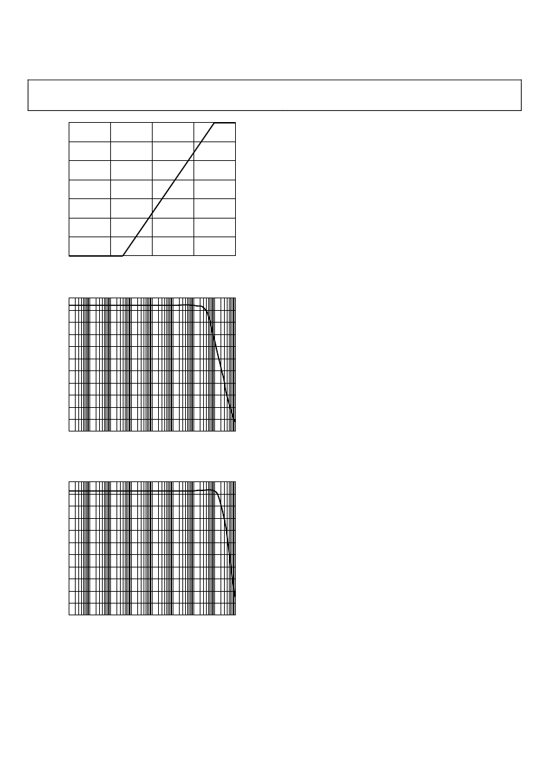
Figure 10. Current Limit
0
0.75
1.00
2.25
2.00
1.25
0.50
0.25
1.50
1.75
2.75
2.50
1
10
100
1k
10k
100k
1M
10M
100M
BANDWIDTH
G
0
Figure 11. V
CMP
Transconductance
0
60
80
180
160
100
40
20
120
140
220
200
1
10
100
1k
10k
100k
1M
10M
100M
BANDWIDTH
G
μ
A
0
Figure 12. C
CMP
and S
CMP
Transconductance
VOLTAGE ERROR AMPLIFIER
This is a high gain transconductance amplifier that takes its
input from the load voltage trim stage described previously. The
amplifier requires only the output pin for loop compensation,
which typically consists of a series RC network-to-common. A
parallel resistor may be added to common to reduce the open-
loop gain and thereby provide some output voltage droop as
output current increases. The output of the amplifier is typically
connected to an emitter follower that drives an optocoupler,
which in turn controls the duty of the primary side PWM. The
emitter follower should have a high gain to minimize loading
effects on the amplifier. Alternatively, an op amp voltage
follower may be used. See Figure 11.
MAIN VOLTAGE REFERENCE
A 1.5 V reference is connected to the inverting input of the
voltage error amplifier. This 1.5 V reference is the output
voltage of the soft-start circuit. Under closed-loop conditions,
the voltage at the noninverting input is also controlled to 1.5 V.
During start-up, the output voltage should be ramped up in a
linear fashion at a rate that is independent of the load current.
This is achieved by digitally ramping up the reference voltage by
using a counter and a DAC. The ramp rate is configurable via
the SMBus. See Figure 13.
CURRENT-SENSE AMPLIFIER
This is a two-stage differential amplifier that achieves low offset
and accuracy. The amplifier has the option to be chopped to
reduce offset or left as a linear amplifier without chopping.
Refer to the Register Listing for more details. The amplifier’s
gain can be selected from three ranges. It is followed by a trim
stage and then by a low gain buffer stage that can be configured
with a gain of 1.0 or 2.1. The result is a total of six overlapping
gain ranges (65 to 230), one of which must be selected via the
SMBus. This gives ample adjustment to compensate for the
poor initial tolerance of the resistance wires typically used for
current sensing. It also allows selecting a higher sensitivity for
better efficiency or a lower sensitivity for better accuracy (lower
offset). The amplifier offset voltage is trimmed to zero in a
once-off operation via the SMBus and uses a voltage-controlled
current source at the output of the first gain stage. A second
controlled current source is used to trim out the additional
offset due to the mismatch of the external divider resistors. This
offset trim is dynamically adjusted according to the common-
mode voltage present at the top of the voltage dividers. Six
ranges are selectable according to the magnitude and polarity of
this offset component. Because the offset compensation circuit
itself has some inaccuracies, the best overall current-sense
accuracy is obtained by using more closely matched external
dividers and then selecting a low compensation range. See
Figure 13.
相关PDF资料 |
PDF描述 |
|---|---|
| ADM1041AARQZ-REEL | Secondary-Side Controller with Current Share and Housekeeping |
| ADM1041AARQZ-REEL7 | Secondary-Side Controller with Current Share and Housekeeping |
| ADM1052 | Precision Dual Voltage Regulator Controller |
| ADM1052JR | Precision Dual Voltage Regulator Controller |
| ADM1060 | DIP Socket; No. of Contacts:56; Pitch Spacing:0.07"; Row Spacing:0.6"; Terminal Type:PC Board; Leaded Process Compatible:Yes; Peak Reflow Compatible (260 C):No RoHS Compliant: Yes |
相关代理商/技术参数 |
参数描述 |
|---|---|
| ADM1041AARQZ-REEL | 功能描述:IC SECONDARY SIDE CTRLR 24QSOP RoHS:是 类别:集成电路 (IC) >> PMIC - 电源控制器,监视器 系列:- 产品培训模块:Lead (SnPb) Finish for COTS Obsolescence Mitigation Program 标准包装:2,500 系列:- 应用:多相控制器 输入电压:- 电源电压:9 V ~ 14 V 电流 - 电源:- 工作温度:-40°C ~ 85°C 安装类型:表面贴装 封装/外壳:40-WFQFN 裸露焊盘 供应商设备封装:40-TQFN-EP(5x5) 包装:带卷 (TR) |
| ADM1041AARQZ-REEL7 | 功能描述:IC SECONDARY SIDE CTRLR 24QSOP RoHS:是 类别:集成电路 (IC) >> PMIC - 电源控制器,监视器 系列:- 产品培训模块:Lead (SnPb) Finish for COTS Obsolescence Mitigation Program 标准包装:2,500 系列:- 应用:多相控制器 输入电压:- 电源电压:9 V ~ 14 V 电流 - 电源:- 工作温度:-40°C ~ 85°C 安装类型:表面贴装 封装/外壳:40-WFQFN 裸露焊盘 供应商设备封装:40-TQFN-EP(5x5) 包装:带卷 (TR) |
| ADM1041A-EVALZ | 功能描述:BOARD EVAL FOR ADM1041A RoHS:是 类别:编程器,开发系统 >> 评估板 - DC/DC 与 AC/DC(离线)SMPS 系列:- 标准包装:1 系列:- 主要目的:DC/DC,步降 输出及类型:1,非隔离 功率 - 输出:- 输出电压:3.3V 电流 - 输出:3A 输入电压:4.5 V ~ 28 V 稳压器拓扑结构:降压 频率 - 开关:250kHz 板类型:完全填充 已供物品:板 已用 IC / 零件:L7981 其它名称:497-12113STEVAL-ISA094V1-ND |
| ADM1041ARQ | 功能描述:IC PWR SUPP MON/LOAD SHAR 24QSOP RoHS:否 类别:集成电路 (IC) >> PMIC - 电源控制器,监视器 系列:- 产品培训模块:Lead (SnPb) Finish for COTS Obsolescence Mitigation Program 标准包装:2,500 系列:- 应用:多相控制器 输入电压:- 电源电压:9 V ~ 14 V 电流 - 电源:- 工作温度:-40°C ~ 85°C 安装类型:表面贴装 封装/外壳:40-WFQFN 裸露焊盘 供应商设备封装:40-TQFN-EP(5x5) 包装:带卷 (TR) |
| ADM1041ARQ-2 | 制造商:Rochester Electronics LLC 功能描述: 制造商:Analog Devices 功能描述: |
发布紧急采购,3分钟左右您将得到回复。