- 您现在的位置:买卖IC网 > PDF目录373995 > ADM1041AARQZ (ANALOG DEVICES INC) Secondary-Side Controller with Current Share and Housekeeping PDF资料下载
参数资料
| 型号: | ADM1041AARQZ |
| 厂商: | ANALOG DEVICES INC |
| 元件分类: | 通信及网络 |
| 英文描述: | Secondary-Side Controller with Current Share and Housekeeping |
| 中文描述: | SPECIALTY TELECOM CIRCUIT, PDSO24 |
| 封装: | LEAD FREE, MO-137AE, QSOP-24 |
| 文件页数: | 31/56页 |
| 文件大小: | 991K |
| 代理商: | ADM1041AARQZ |
第1页第2页第3页第4页第5页第6页第7页第8页第9页第10页第11页第12页第13页第14页第15页第16页第17页第18页第19页第20页第21页第22页第23页第24页第25页第26页第27页第28页第29页第30页当前第31页第32页第33页第34页第35页第36页第37页第38页第39页第40页第41页第42页第43页第44页第45页第46页第47页第48页第49页第50页第51页第52页第53页第54页第55页第56页
ADM1041A
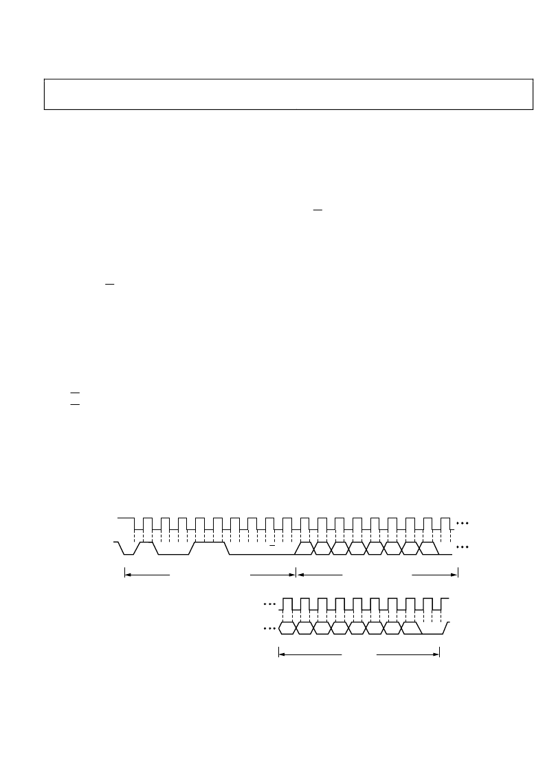
GENERAL SMBus TIMING
The SMBus specification defines specific conditions for
different types of read and write operations. General SMBus
read and write operations are shown in the timing diagrams of
Figure 25, Figure 26, and Figure 27, and described in the
following sections.
Rev. 0 | Page 31 of 56
The general SMBus protocol operates as follows.
The master initiates data transfer by establishing a start
condition, defined as a high-to-low transition on the serial data
line, SDA, while the serial clock line, SCL, remains high. This
indicates that a data stream follows. All slave peripherals
connected to the serial bus respond to the start condition and
shift in the next 8 bits, consisting of a 7-bit slave address (MSB
first), plus an R/W bit, which determines the direction of the
data transfer, that is, whether data is written to or read from the
slave device (0 = write, 1 = read).
The peripheral whose address corresponds to the transmitted
address responds by pulling the data line low during the low
period before the ninth clock pulse, known as the Acknowledge
bit, and holding it low during the high period of this clock
pulse. All other devices on the bus remain idle while the
selected device waits for data to be read from or written to it. If
the R/W bit is a 0, then the master writes to the slave device. If
the R/W bit is a 1, the master reads from the slave device.
Data is sent over the serial bus in sequences of nine clock
pulses, eight bits of data, followed by an Acknowledge bit from
the slave device. Data transitions on the data line must occur
during the low period of the clock signal and remain stable
during the high period, because a low-to-high transition when
the clock is high may be interpreted as a stop signal.
If the operation is a write operation, the first data byte after the
slave address is a command byte. This tells the slave device what
to expect next. It may be an instruction, such as telling the slave
device to expect a block write, or it may be a register address
that tells the slave where subsequent data is to be written.
Because data can flow in only one direction as defined by the
R/W bit, it is not possible to send a command to a slave device
during a read operation. Before doing a read operation, it might
first be necessary to perform a write operation to tell the slave
what sort of read operation to expect and/or the address from
which data is to be read.
When all data bytes have been read or written, stop conditions
are established. In write mode, the master pulls the SDA line
high during the tenth clock pulse to assert a stop condition. In
read mode, the master device releases the SDA line during the
low period before the ninth clock pulse, but the slave device
does not pull it low. This is known as No Acknowledge. The
master then takes the data line low during the low period before
the tenth clock pulse, then high during the tenth clock pulse to
assert a stop condition.
Note:
If it is required to perform several read or write
operations in succession, the master can send a repeat start
condition instead of a stop condition to begin a new operation.
START BY
MASTER
STOP BY
MASTER
ACK. BY
ADM1041A
ACK. BY
ADM1041A
ACK. BY
ADM1041A
A6
19
1
9
9
A5
A4
A3
A2
A1
A0
R/W
D7
D6
D5
D4
D3
D2
D1
D0
SCLK
SDATA
FRAME 1
SERIAL BUS ADDRESS BYTE
FRAME 2
ADDRESS POINTER REGISTER BYTE
FRAME 3
DATA BYTE
SDATA (CONTINUED)
SCLK (CONTINUED)
9
1
D7
D6
D5
D4
D3
D2
D1
D0
0
Figure 25. Writing a Register Address to the Address Pointer Register, then Writing Data to the Selected Register
相关PDF资料 |
PDF描述 |
|---|---|
| ADM1041AARQZ-REEL | Secondary-Side Controller with Current Share and Housekeeping |
| ADM1041AARQZ-REEL7 | Secondary-Side Controller with Current Share and Housekeeping |
| ADM1052 | Precision Dual Voltage Regulator Controller |
| ADM1052JR | Precision Dual Voltage Regulator Controller |
| ADM1060 | DIP Socket; No. of Contacts:56; Pitch Spacing:0.07"; Row Spacing:0.6"; Terminal Type:PC Board; Leaded Process Compatible:Yes; Peak Reflow Compatible (260 C):No RoHS Compliant: Yes |
相关代理商/技术参数 |
参数描述 |
|---|---|
| ADM1041AARQZ-REEL | 功能描述:IC SECONDARY SIDE CTRLR 24QSOP RoHS:是 类别:集成电路 (IC) >> PMIC - 电源控制器,监视器 系列:- 产品培训模块:Lead (SnPb) Finish for COTS Obsolescence Mitigation Program 标准包装:2,500 系列:- 应用:多相控制器 输入电压:- 电源电压:9 V ~ 14 V 电流 - 电源:- 工作温度:-40°C ~ 85°C 安装类型:表面贴装 封装/外壳:40-WFQFN 裸露焊盘 供应商设备封装:40-TQFN-EP(5x5) 包装:带卷 (TR) |
| ADM1041AARQZ-REEL7 | 功能描述:IC SECONDARY SIDE CTRLR 24QSOP RoHS:是 类别:集成电路 (IC) >> PMIC - 电源控制器,监视器 系列:- 产品培训模块:Lead (SnPb) Finish for COTS Obsolescence Mitigation Program 标准包装:2,500 系列:- 应用:多相控制器 输入电压:- 电源电压:9 V ~ 14 V 电流 - 电源:- 工作温度:-40°C ~ 85°C 安装类型:表面贴装 封装/外壳:40-WFQFN 裸露焊盘 供应商设备封装:40-TQFN-EP(5x5) 包装:带卷 (TR) |
| ADM1041A-EVALZ | 功能描述:BOARD EVAL FOR ADM1041A RoHS:是 类别:编程器,开发系统 >> 评估板 - DC/DC 与 AC/DC(离线)SMPS 系列:- 标准包装:1 系列:- 主要目的:DC/DC,步降 输出及类型:1,非隔离 功率 - 输出:- 输出电压:3.3V 电流 - 输出:3A 输入电压:4.5 V ~ 28 V 稳压器拓扑结构:降压 频率 - 开关:250kHz 板类型:完全填充 已供物品:板 已用 IC / 零件:L7981 其它名称:497-12113STEVAL-ISA094V1-ND |
| ADM1041ARQ | 功能描述:IC PWR SUPP MON/LOAD SHAR 24QSOP RoHS:否 类别:集成电路 (IC) >> PMIC - 电源控制器,监视器 系列:- 产品培训模块:Lead (SnPb) Finish for COTS Obsolescence Mitigation Program 标准包装:2,500 系列:- 应用:多相控制器 输入电压:- 电源电压:9 V ~ 14 V 电流 - 电源:- 工作温度:-40°C ~ 85°C 安装类型:表面贴装 封装/外壳:40-WFQFN 裸露焊盘 供应商设备封装:40-TQFN-EP(5x5) 包装:带卷 (TR) |
| ADM1041ARQ-2 | 制造商:Rochester Electronics LLC 功能描述: 制造商:Analog Devices 功能描述: |
发布紧急采购,3分钟左右您将得到回复。