- 您现在的位置:买卖IC网 > PDF目录373995 > ADM1060 (Analog Devices, Inc.) DIP Socket; No. of Contacts:56; Pitch Spacing:0.07"; Row Spacing:0.6"; Terminal Type:PC Board; Leaded Process Compatible:Yes; Peak Reflow Compatible (260 C):No RoHS Compliant: Yes PDF资料下载
参数资料
| 型号: | ADM1060 |
| 厂商: | Analog Devices, Inc. |
| 英文描述: | DIP Socket; No. of Contacts:56; Pitch Spacing:0.07"; Row Spacing:0.6"; Terminal Type:PC Board; Leaded Process Compatible:Yes; Peak Reflow Compatible (260 C):No RoHS Compliant: Yes |
| 中文描述: | 通信系统监控/排序电路 |
| 文件页数: | 40/45页 |
| 文件大小: | 303K |
| 代理商: | ADM1060 |
第1页第2页第3页第4页第5页第6页第7页第8页第9页第10页第11页第12页第13页第14页第15页第16页第17页第18页第19页第20页第21页第22页第23页第24页第25页第26页第27页第28页第29页第30页第31页第32页第33页第34页第35页第36页第37页第38页第39页当前第40页第41页第42页第43页第44页第45页
ADM1060
PROGRAMMNGADM1060
–
40
–
REV. PrJ 11/02
PRELIMINARY TECHNICAL DATA
SMBUS PR OT OC OL S F OR R AM AND E E PR OM
T he ADM1060 contains volatile registers (RAM) and
non-volatile EEPROM. User RAM occupies address loca-
tions from 00h to DFh, whilst EEPROM occupies ad-
dresses from F800h to F9FFh.
Data can be written to and read from both RAM and
EEPROM as single data bytes.
Data can only be written to unprogrammed EEPROM
locations. T o write new data to a programmed location it
is first necessary to erase it. EEPROM erasure cannot be
done at the byte level, the EEPROM is arranged as 16
pages of 32 bytes, and an entire page must be erased.
Page erasure is enabled by setting bit 3 in register
UPDCFG (address 90h) to 1. If this is not set then page
erasure cannot occur, even if the command byte (FEh) is
programmed across the SMBus.
A D M1060 WR IT E OPE R A T IONS
T he SMBus specification defines several protocols for
different types of read and write operations. T he ones used
in the ADM1060 are discussed below. T he following ab-
breviations are used in the diagrams:
S
-
ST AR T
P
-
ST OP
R
-
R E AD
W
-
W R IT E
A
-
A C K N OW L E D G E
A
-
NO AC K NOWL E D G E
T he ADM1060 uses the following SMBus write protocols:
Send Byte
In this operation the master device sends a single com-
mand byte to a slave device, as follows:
1. T he master device asserts a start condition on SDA.
2. T he master sends the 7-bit slave address followed by
the write bit (low).
3. T he addressed slave device asserts ACK on SDA.
4. T he master sends a command code.
5. T he slave asserts ACK on SDA.
6. T he master asserts a ST OP condition on SDA and the
transaction ends.
In the ADM1060, the send byte protocol is used for two
purposes.
1. T o write a register address to RAM for a subsequent
single byte read from the same address or block read or
write starting at that address. T his is illustrated in Figure
9a.
S
ASLAVE
RAM
ADDRESS
(00h TO DFh)
A P
1
2
3
4
5
6
Figure 9a. Setting A RAM Address For Subsequent Read
3. Erase a page of EEPROM memory. EEPROM
memory can be written to only if it is unprogrammed.
Before writing to one or more EEPROM memory
locations that are already programmed, the page or
pages containing those locations must first be erased.
EEPROM memory is erased by writing a command
byte.
T he master sends a command code that tells the slave
device to erase the page. T he ADM1060 command
code for a pages(s) erasure is FEh (11111110). Note
that, in order for page erasure to take place, the page
address has to be given in the previous write word
transaction (see write byte below). Also, bit 3 in regis-
ter UPDCFG (address 90h) must be set to 1.
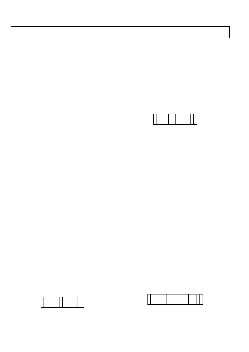
S
ASLAVE
COMMAND
BYTE
(FEh)
A P
1
2
3
4
5
6
Figure 9b. EEPROM Page Erasure
As soon as the ADM1060 receives the command byte,
page erasure begins. T he master device can send a
ST OP command as soon as it sends the command
byte. Page erasure takes approximately 20ms. If the
ADM1060 is accessed before erasure is complete, it
will respond with No Acknowledge.
Write Byte/Word
In this operation the master device sends a command byte
and one or two data bytes to the slave device, as follows:
1. T he master device asserts a start condition on SDA.
2. T he master sends the 7-bit slave address followed by
the write bit (low).
3. T he addressed slave device asserts ACK on SDA.
4. T he master sends a command code.
5. T he slave asserts ACK on SDA.
6. T he master sends a data byte.
7. T he slave asserts ACK on SDA.
8. T he master sends a data byte (or may assert ST OP at
this point).
9. T he slave asserts ACK on SDA.
10.T he master asserts a ST OP condition on SDA to end
the transaction.
In the ADM1060, the write byte/word protocol is used for
three purposes.
1. Write a single byte of data to RAM. In this case the
command byte is the RAM address from 00h to DFh
and the (only) data byte is the actual data. T his is illus-
trated in Figure 9c.
S
SLAVE
ADDRESS
W
A
RAM
ADDRESS
(00h TO DFh)
A DATA A P
1
2
3
4
5
6
7
8
Figure 9c. Single Byte Write To RAM
2. Set up a two byte EEPROM address for a subsequent
read, write, block read, block write or page erase. In
相关PDF资料 |
PDF描述 |
|---|---|
| ADM1060ARU | CON-HDR64POS2ROW 4WALL.1X.1SP,RTANG,LOPF |
| ADM1064 | Super Sequencer with Voltage Readback ADC |
| ADM1064ACP | Super Sequencer with Voltage Readback ADC |
| ADM1064ACP-REEL | Super Sequencer with Voltage Readback ADC |
| ADM1064ACP-REEL7 | Super Sequencer with Voltage Readback ADC |
相关代理商/技术参数 |
参数描述 |
|---|---|
| ADM1060ARU | 功能描述:IC SUPERVIS/SEQUENC 7-CH 28TSSOP RoHS:否 类别:集成电路 (IC) >> PMIC - 监控器 系列:Super Sequencer® 标准包装:1 系列:- 类型:简单复位/加电复位 监视电压数目:1 输出:开路漏极或开路集电极 复位:高有效 复位超时:- 电压 - 阀值:1.8V 工作温度:-40°C ~ 125°C 安装类型:表面贴装 封装/外壳:6-TSOP(0.059",1.50mm 宽)5 引线 供应商设备封装:5-TSOP 包装:剪切带 (CT) 其它名称:NCP301HSN18T1GOSCT |
| ADM1060ARUCS0001R7 | 功能描述:IC SUPERVISOR/SEQUENCER 制造商:analog devices inc. 系列:* 零件状态:上次购买时间 标准包装:1 |
| ADM1060ARUCS0100R7 | 功能描述:IC SUPERVISOR/SEQUENCER 制造商:analog devices inc. 系列:* 零件状态:上次购买时间 标准包装:1 |
| ADM1060ARUCS0101R7 | 功能描述:IC SUPERVISOR/SEQUENCER 制造商:analog devices inc. 系列:* 零件状态:上次购买时间 标准包装:1 |
| ADM1060ARUCS0102R7 | 功能描述:IC SUPERVISOR/SEQUENCER 制造商:analog devices inc. 系列:* 零件状态:上次购买时间 标准包装:1 |
发布紧急采购,3分钟左右您将得到回复。