- 您现在的位置:买卖IC网 > PDF目录373996 > ADM1069ACP (Analog Devices, Inc.) SUPER SEQUENCER-TM WITH MARGINING CONTROL AND AUXILIARY ADC INPUTS PDF资料下载
参数资料
| 型号: | ADM1069ACP |
| 厂商: | Analog Devices, Inc. |
| 英文描述: | SUPER SEQUENCER-TM WITH MARGINING CONTROL AND AUXILIARY ADC INPUTS |
| 中文描述: | 超时序与裕度控制以及辅助ADC输入商标 |
| 文件页数: | 29/32页 |
| 文件大小: | 626K |
| 代理商: | ADM1069ACP |
第1页第2页第3页第4页第5页第6页第7页第8页第9页第10页第11页第12页第13页第14页第15页第16页第17页第18页第19页第20页第21页第22页第23页第24页第25页第26页第27页第28页当前第29页第30页第31页第32页
Preliminary Technical Data
ADM1069
5.
Rev. PrB | Page 29 of 32
The slave asserts ACK on SDA.
6.
The master sends a data byte that tells the slave device how
many data bytes are being sent. The SMBus specification
allows a maximum of 32 data bytes in a block write.
7.
The slave asserts ACK on SDA.
8.
The master sends N data bytes.
9.
The slave asserts ACK on SDA after each data byte.
10.
The master asserts a stop condition on SDA to end the
transaction.
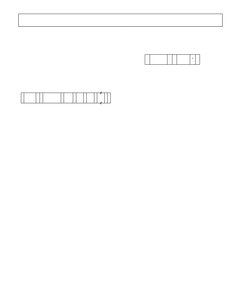
0
ASLAVE
S
W A
2
(BLOCK WRITE)
4
1
3
A
5
BYTE
6
A
7
A
9
10
A
P
A
D1
8
DN
D2
Figure 43. Block Write to EEPROM or RAM
Unlike some EEPROM devices that limit block writes to within
a page boundary, there is no limitation on the start address
when performing a block write to EEPROM, except
There must be at least N locations from the start address to
the highest EEPROM address (0xFBFF), to avoid writing to
invalid addresses.
If the addresses cross a page boundary, both pages must be
erased before programming.
Note that the ADM1069 features a clock extend function for
writes to EEPROM. Programming an EEPROM byte takes
approximately 250 μs, which would limit the SMBus clock for
repeated or block write operations. The ADM1069 pulls SCL
low and extends the clock pulse when it cannot accept any
more data.
READ OPERATIONS
The ADM1069 uses the following SMBus read protocols.
Receive Byte
In a receive byte operation, the master device receives a single
byte from a slave device, as follows:
1.
The master device asserts a start condition on SDA.
2.
The master sends the 7-bit slave address followed by the
read bit (high).
3.
The addressed slave device asserts ACK on SDA.
4.
The master receives a data byte.
5.
The master asserts no acknowledge on SDA.
6.
The master asserts a stop condition on SDA, and the
transaction ends.
In the ADM1069, the receive byte protocol is used to read a
single byte of data from a RAM or EEPROM location whose
address has previously been set by a send byte or write
byte/word operation, as shown in Figure 44.
0
2
3
1
4
5
SLAVE
ADDRESS
S
R
DATA
P
A
6
A
Figure 44. Single Byte Read from EEPROM or RAM
Block Read
In a block read operation, the master device reads a block of
data from a slave device. The start address for a block read must
have been set previously. In the ADM1069, this is done by a
send byte operation to set a RAM address, or a write byte/word
operation to set an EEPROM address. The block read operation
itself consists of a send byte operation that sends a block read
command to the slave, immediately followed by a repeated start
and a read operation that reads out multiple data bytes, as
follows:
1.
The master device asserts a start condition on SDA.
2.
The master sends the 7-bit slave address followed by the
write bit (low).
3.
The addressed slave device asserts ACK on SDA.
4.
The master sends a command code that tells the slave
device to expect a block read. The ADM1069 command
code for a block read is 0xFD (1111 1101).
5.
The slave asserts ACK on SDA.
6.
The master asserts a repeat start condition on SDA.
7.
The master sends the 7-bit slave address followed by the
read bit (high).
8.
The slave asserts ACK on SDA.
9.
The ADM1069 sends a byte-count data byte that tells the
master how many data bytes to expect. The ADM1069
always returns 32 data bytes (0x20), which is the maximum
allowed by the SMBus 1.1 specification.
10.
The master asserts ACK on SDA.
11.
The master receives 32 data bytes.
12.
The master asserts ACK on SDA after each data byte.
13.
The master asserts a stop condition on SDA to end the
transaction.
相关PDF资料 |
PDF描述 |
|---|---|
| ADM1069ACP-REEL | SUPER SEQUENCER-TM WITH MARGINING CONTROL AND AUXILIARY ADC INPUTS |
| ADM1069ACP-REEL7 | SUPER SEQUENCER-TM WITH MARGINING CONTROL AND AUXILIARY ADC INPUTS |
| ADM1070 | -48 V Hot Swap Controller |
| ADM1070ART | -48 V Hot Swap Controller |
| ADM1072ARQ | Dual, USB 2.0 Full/Standby Power Controller with Supply Steering |
相关代理商/技术参数 |
参数描述 |
|---|---|
| ADM1069ACP-REEL | 制造商:AD 制造商全称:Analog Devices 功能描述:SUPER SEQUENCER-TM WITH MARGINING CONTROL AND AUXILIARY ADC INPUTS |
| ADM1069ACP-REEL7 | 制造商:AD 制造商全称:Analog Devices 功能描述:SUPER SEQUENCER-TM WITH MARGINING CONTROL AND AUXILIARY ADC INPUTS |
| ADM1069ACPZ | 功能描述:IC SUPERVISOR/SEQ PROG 40LFCSP RoHS:是 类别:集成电路 (IC) >> PMIC - 监控器 系列:Super Sequencer® 其它有关文件:STM6717 View All Specifications 标准包装:1 系列:- 类型:多压监控器 监视电压数目:2 输出:开路漏极或开路集电极 复位:低有效 复位超时:最小为 600 ms 电压 - 阀值:1.11V,3.075V 工作温度:-40°C ~ 85°C 安装类型:表面贴装 封装/外壳:SC-74A,SOT-753 供应商设备封装:SOT-23-5 包装:Digi-Reel® 产品目录页面:1194 (CN2011-ZH PDF) 其它名称:497-7019-6 |
| ADM1069ACPZ-REEL | 功能描述:IC SUPERVISOR/SEQ PROG 40LFCSP RoHS:是 类别:集成电路 (IC) >> PMIC - 监控器 系列:Super Sequencer® 标准包装:1 系列:- 类型:简单复位/加电复位 监视电压数目:1 输出:开路漏极或开路集电极 复位:高有效 复位超时:- 电压 - 阀值:1.8V 工作温度:-40°C ~ 125°C 安装类型:表面贴装 封装/外壳:6-TSOP(0.059",1.50mm 宽)5 引线 供应商设备封装:5-TSOP 包装:剪切带 (CT) 其它名称:NCP301HSN18T1GOSCT |
| ADM1069ACPZ-REEL7 | 功能描述:IC SUPERVISOR/SEQ PROG 40LFCSP RoHS:是 类别:集成电路 (IC) >> PMIC - 监控器 系列:Super Sequencer® 标准包装:1 系列:- 类型:简单复位/加电复位 监视电压数目:1 输出:开路漏极或开路集电极 复位:高有效 复位超时:- 电压 - 阀值:1.8V 工作温度:-40°C ~ 125°C 安装类型:表面贴装 封装/外壳:6-TSOP(0.059",1.50mm 宽)5 引线 供应商设备封装:5-TSOP 包装:剪切带 (CT) 其它名称:NCP301HSN18T1GOSCT |
发布紧急采购,3分钟左右您将得到回复。