- 您现在的位置:买卖IC网 > PDF目录373996 > ADM1069ACP (Analog Devices, Inc.) SUPER SEQUENCER-TM WITH MARGINING CONTROL AND AUXILIARY ADC INPUTS PDF资料下载
参数资料
| 型号: | ADM1069ACP |
| 厂商: | Analog Devices, Inc. |
| 英文描述: | SUPER SEQUENCER-TM WITH MARGINING CONTROL AND AUXILIARY ADC INPUTS |
| 中文描述: | 超时序与裕度控制以及辅助ADC输入商标 |
| 文件页数: | 7/32页 |
| 文件大小: | 626K |
| 代理商: | ADM1069ACP |
第1页第2页第3页第4页第5页第6页当前第7页第8页第9页第10页第11页第12页第13页第14页第15页第16页第17页第18页第19页第20页第21页第22页第23页第24页第25页第26页第27页第28页第29页第30页第31页第32页
Preliminary Technical Data
ADM1069
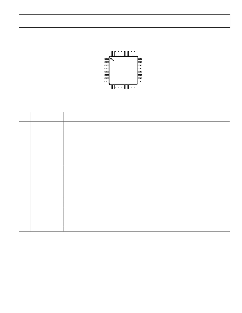
PIN CONFIGURATION AND FUNCTION DESCRIPTIONS
Rev. PrB | Page 7 of 32
0
1
25
32
8
9
17
16
24
VX1
VX2
VX3
VX4
VP1
VP2
VP3
VH
PDO1
PDO2
PDO3
PDO4
PDO5
PDO6
PDO7
PDO8
G
V
S
S
A
A
V
P
A
R
R
R
D
D
D
D
PIN 1
ADM1069
TOP VIEW
(Not to Scale)
Figure 3. LQFP Pin Configuration
Table 2. Pin Function Descriptions
Pin
No.
Mnemonic
1–4
VX1–4
Description
High Impedance Inputs to Supply Fault Detectors. Fault thresholds can be set from 0.573 V to 1.375 V.
Alternatively, these pins can be used as general-purpose digital inputs.
Low Voltage Inputs to Supply Fault Detectors. Three input ranges can be set by altering the input attenuation
on a potential divider connected to these pins, the output of which connects to a supply fault detector. These
pins allow thresholds from 2.5 V to 6.0 V, 1.25 V to 3.00 V, and 0.573 V to 1.375 V.
High Voltage Input to Supply Fault Detectors. Three input ranges can be set by altering the input attenuation
on a potential divider connected to this pin, the output of which connects to a supply fault detector. This pin
allows thresholds from 6.0 V to 14.4 V and 2.5 V to 6.0 V.
Ground Return for Input Attenuators.
Ground Return for On-Chip Reference Circuits.
Reference Input for ADC. Nominally, 2.048V.
2.048 V Reference Output.
Voltage Output DACs. These pins default to high impedance at power-up.
5–7
VP1–3
8
VH
9
10
11
12
13-
16
17-
24
25
26
27
28
29
30
31
32
AGND
REFGND
REFIN
REFOUT
DAC1-4
PDO8–1
Programmable Output Drivers.
PDOGND
VCCP
A0
A1
SCL
SDA
VDDCAP
GND
Ground Return for Output Drivers.
Central Charge-Pump Voltage of 5.25 V. A reservoir capacitor must be connected between this pin and GND.
Logic Input. This pin sets the seventh bit of the SMBus interface address.
Logic Input. This pin sets the sixth bit of the SMBus interface address.
SMBus Clock Pin. Open-drain output requires external resistive pull-up.
SMBus Data I/O Pin. Open-drain output requires external resistive pull-up.
Device Supply Voltage. Linearly regulated from the highest of the VP1–3, VH pins to a typical of 4.75 V.
Supply Ground.
相关PDF资料 |
PDF描述 |
|---|---|
| ADM1069ACP-REEL | SUPER SEQUENCER-TM WITH MARGINING CONTROL AND AUXILIARY ADC INPUTS |
| ADM1069ACP-REEL7 | SUPER SEQUENCER-TM WITH MARGINING CONTROL AND AUXILIARY ADC INPUTS |
| ADM1070 | -48 V Hot Swap Controller |
| ADM1070ART | -48 V Hot Swap Controller |
| ADM1072ARQ | Dual, USB 2.0 Full/Standby Power Controller with Supply Steering |
相关代理商/技术参数 |
参数描述 |
|---|---|
| ADM1069ACP-REEL | 制造商:AD 制造商全称:Analog Devices 功能描述:SUPER SEQUENCER-TM WITH MARGINING CONTROL AND AUXILIARY ADC INPUTS |
| ADM1069ACP-REEL7 | 制造商:AD 制造商全称:Analog Devices 功能描述:SUPER SEQUENCER-TM WITH MARGINING CONTROL AND AUXILIARY ADC INPUTS |
| ADM1069ACPZ | 功能描述:IC SUPERVISOR/SEQ PROG 40LFCSP RoHS:是 类别:集成电路 (IC) >> PMIC - 监控器 系列:Super Sequencer® 其它有关文件:STM6717 View All Specifications 标准包装:1 系列:- 类型:多压监控器 监视电压数目:2 输出:开路漏极或开路集电极 复位:低有效 复位超时:最小为 600 ms 电压 - 阀值:1.11V,3.075V 工作温度:-40°C ~ 85°C 安装类型:表面贴装 封装/外壳:SC-74A,SOT-753 供应商设备封装:SOT-23-5 包装:Digi-Reel® 产品目录页面:1194 (CN2011-ZH PDF) 其它名称:497-7019-6 |
| ADM1069ACPZ-REEL | 功能描述:IC SUPERVISOR/SEQ PROG 40LFCSP RoHS:是 类别:集成电路 (IC) >> PMIC - 监控器 系列:Super Sequencer® 标准包装:1 系列:- 类型:简单复位/加电复位 监视电压数目:1 输出:开路漏极或开路集电极 复位:高有效 复位超时:- 电压 - 阀值:1.8V 工作温度:-40°C ~ 125°C 安装类型:表面贴装 封装/外壳:6-TSOP(0.059",1.50mm 宽)5 引线 供应商设备封装:5-TSOP 包装:剪切带 (CT) 其它名称:NCP301HSN18T1GOSCT |
| ADM1069ACPZ-REEL7 | 功能描述:IC SUPERVISOR/SEQ PROG 40LFCSP RoHS:是 类别:集成电路 (IC) >> PMIC - 监控器 系列:Super Sequencer® 标准包装:1 系列:- 类型:简单复位/加电复位 监视电压数目:1 输出:开路漏极或开路集电极 复位:高有效 复位超时:- 电压 - 阀值:1.8V 工作温度:-40°C ~ 125°C 安装类型:表面贴装 封装/外壳:6-TSOP(0.059",1.50mm 宽)5 引线 供应商设备封装:5-TSOP 包装:剪切带 (CT) 其它名称:NCP301HSN18T1GOSCT |
发布紧急采购,3分钟左右您将得到回复。