- 您现在的位置:买卖IC网 > PDF目录210168 > ADM1069AST-REEL7 (ANALOG DEVICES INC) 8-CHANNEL POWER SUPPLY SUPPORT CKT, PQFP32 PDF资料下载
参数资料
| 型号: | ADM1069AST-REEL7 |
| 厂商: | ANALOG DEVICES INC |
| 元件分类: | 电源管理 |
| 英文描述: | 8-CHANNEL POWER SUPPLY SUPPORT CKT, PQFP32 |
| 封装: | MS-026-BBA, LQFP-32 |
| 文件页数: | 16/36页 |
| 文件大小: | 763K |
| 代理商: | ADM1069AST-REEL7 |
第1页第2页第3页第4页第5页第6页第7页第8页第9页第10页第11页第12页第13页第14页第15页当前第16页第17页第18页第19页第20页第21页第22页第23页第24页第25页第26页第27页第28页第29页第30页第31页第32页第33页第34页第35页第36页
ADM1069
Rev. A | Page 23 of 36
SUPPLY MARGINING
OVERVIEW
It is often necessary for the system designer to adjust supplies,
either to optimize their level or force them away from nominal
values to characterize the system performance under these
conditions. This is a function typically performed during an in-
circuit test (ICT), such as the manufacturer wants to guarantee
that the product under test functions correctly at nominal
supplies minus 10%.
OPEN-LOOP MARGINING
The simplest method of margining a supply is to implement an
open-loop technique. A popular method for this is to switch extra
resistors into the feedback node of a power module, such as a
dc-to-dc converter or low dropout regulator (LDO). The extra
resistor alters the voltage at the feedback or trim node and forces
the output voltage to margin up or down by a certain amount.
The ADM1069 can perform open-loop margining for up to four
supplies. The four on-board voltage DACs (DAC1 to DAC4)
can drive into the feedback pins of the power modules to be
margined. The simplest circuit to implement this function is an
attenuation resistor, which connects the DACn pin to the
feedback node of a dc-to-dc converter. When the DACn output
voltage is set equal to the feedback voltage, no current flows in
the attenuation resistor, and the dc-to-dc output voltage does
not change. Taking DACn above the feedback voltage forces
current into the feedback node, and the output of the dc-to-dc
converter is forced to fall to compensate for this. The dc-to-dc
output can be forced high by setting the DACn output voltage
lower than the feedback node voltage. The series resistor can be
split in two, and the node between them can be decoupled with
a capacitor to ground. This can help to decouple any noise
picked up from the board. Decoupling to a ground local to the
dc-to-dc converter is recommended.
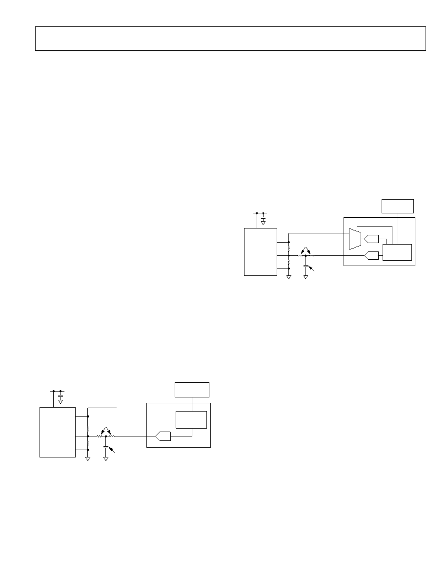
04735-067
OUTPUT
DC/DC
CONVERTER
FEEDBACK
GND
ATTENUATION
RESISTOR
PCB
TRACE NOISE
DECOUPLING
CAPACITOR
ADM1069
DACOUTn
VOUT
DAC
μCONTROLLER
VIN
DEVICE
CONTROLLER
(SMBus)
Figure 31. Open-Loop Margining System Using the ADM1069
The ADM1069 can be commanded to margin a supply up or
down over the SMBus by updating the values on the relevant
DAC output.
CLOSED-LOOP SUPPLY MARGINING
A more accurate and comprehensive method of margining is to
implement a closed-loop system. The voltage on the rail to be
margined can be read back to accurately margin the rail to the
target voltage. The ADM1069 incorporates all the circuits
required to do this, with its 12-bit successive approximation
ADC used to read back the level of supervised voltages, and its
six voltage output DACs, implemented as described in the
Open-Loop Margining section, used to adjust supply levels.
These circuits can be used along with some other intelligence
such as a microcontroller to implement a closed-loop margin-
ing system that allows any dc-to-dc converter or LDO supply to
be set to any voltage, accurate to within ±0.5% of the target.
04735-
034
OUTPUT
DC/DC
CONVERTER
FEEDBACK
GND
ATTENUATION
RESISTOR
PCB
TRACE NOISE
DECOUPLING
CAPACITOR
VH/VPn/VXn
ADM1069
DACOUTn
MUX
ADC
DAC
DEVICE
CONTROLLER
(SMBus)
μCONTROLLER
VIN
Figure 32. Closed-Loop Margining System Using the ADM1069
To implement closed-loop margining:
1.
Disable the four DACn outputs.
2.
Set the DAC output voltage equal to the voltage on the
feedback node.
3.
Enable the DAC.
4.
Read the voltage at the dc-to-dc output that is connected to
one of the VPn, VH, or VXn pins.
5.
If necessary, modify the DACn output code up or down to
adjust the dc-to-dc output voltage. Otherwise, stop because
the target voltage has been reached.
6.
Set the DAC output voltage to a value that alters the supply
output by the required amount (for example, ±5%).
7.
Repeat from Step 4.
Step 1 to Step 3 ensure that when the DACn output buffer is
turned on it has little effect on the dc-to-dc converter output. The
DAC output buffer is designed to power up without glitching by
first powering up the buffer to follow the pin voltage. It does not
drive out onto the pin at this time. Once the output buffer is
properly enabled, the buffer input is switched over to the DAC,
and the output stage of the buffer is turned on. Output glitching
is negligible.
相关PDF资料 |
PDF描述 |
|---|---|
| AFL27005DX/CHPBF | 2-OUTPUT 66 W DC-DC REG PWR SUPPLY MODULE |
| AFL27012DX/CHPBF | 2-OUTPUT 66 W DC-DC REG PWR SUPPLY MODULE |
| APE2902Y5-46 | SWITCHING REGULATOR, PDSO5 |
| APE2902Y5R-49 | SWITCHING REGULATOR, PDSO5 |
| ATW2805S/-SLV | 1-OUTPUT 30 W DC-DC REG PWR SUPPLY MODULE |
相关代理商/技术参数 |
参数描述 |
|---|---|
| ADM1069ASTZ | 功能描述:IC SUPERVISOR/SEQUENCER 32-LQFP RoHS:是 类别:集成电路 (IC) >> PMIC - 监控器 系列:Super Sequencer® 其它有关文件:STM6905 View All Specifications 标准包装:1 系列:- 类型:多压监控器 监视电压数目:5 输出:开路漏极或开路集电极 复位:低有效 复位超时:最小为 140 ms 电压 - 阀值:2.188V,2.955V,可调,可调,可调 工作温度:-40°C ~ 85°C 安装类型:表面贴装 封装/外壳:8-TSSOP,8-MSOP(0.118",3.00mm 宽) 供应商设备封装:8-TSSOP 包装:Digi-Reel® 产品目录页面:1197 (CN2011-ZH PDF) 其它名称:497-8728-6 |
| ADM1069ASTZ-REEL | 功能描述:IC SEQUENCER/SUPERVISOR 32LQFP RoHS:是 类别:集成电路 (IC) >> PMIC - 监控器 系列:Super Sequencer® 标准包装:1 系列:- 类型:简单复位/加电复位 监视电压数目:1 输出:开路漏极或开路集电极 复位:高有效 复位超时:- 电压 - 阀值:1.8V 工作温度:-40°C ~ 125°C 安装类型:表面贴装 封装/外壳:6-TSOP(0.059",1.50mm 宽)5 引线 供应商设备封装:5-TSOP 包装:剪切带 (CT) 其它名称:NCP301HSN18T1GOSCT |
| ADM1069ASTZ-REEL7 | 功能描述:IC SEQUENCER/SUPERVISOR 32LQFP RoHS:是 类别:集成电路 (IC) >> PMIC - 监控器 系列:Super Sequencer® 其它有关文件:STM6905 View All Specifications 标准包装:1 系列:- 类型:多压监控器 监视电压数目:5 输出:开路漏极或开路集电极 复位:低有效 复位超时:最小为 140 ms 电压 - 阀值:2.188V,2.955V,可调,可调,可调 工作温度:-40°C ~ 85°C 安装类型:表面贴装 封装/外壳:8-TSSOP,8-MSOP(0.118",3.00mm 宽) 供应商设备封装:8-TSSOP 包装:Digi-Reel® 产品目录页面:1197 (CN2011-ZH PDF) 其它名称:497-8728-6 |
| ADM1070 | 制造商:AD 制造商全称:Analog Devices 功能描述:-48 V Hot Swap Controller |
| ADM1070ART | 制造商:AD 制造商全称:Analog Devices 功能描述:-48 V Hot Swap Controller |
发布紧急采购,3分钟左右您将得到回复。