- 您现在的位置:买卖IC网 > PDF目录210168 > ADM1069AST-REEL7 (ANALOG DEVICES INC) 8-CHANNEL POWER SUPPLY SUPPORT CKT, PQFP32 PDF资料下载
参数资料
| 型号: | ADM1069AST-REEL7 |
| 厂商: | ANALOG DEVICES INC |
| 元件分类: | 电源管理 |
| 英文描述: | 8-CHANNEL POWER SUPPLY SUPPORT CKT, PQFP32 |
| 封装: | MS-026-BBA, LQFP-32 |
| 文件页数: | 6/36页 |
| 文件大小: | 763K |
| 代理商: | ADM1069AST-REEL7 |
第1页第2页第3页第4页第5页当前第6页第7页第8页第9页第10页第11页第12页第13页第14页第15页第16页第17页第18页第19页第20页第21页第22页第23页第24页第25页第26页第27页第28页第29页第30页第31页第32页第33页第34页第35页第36页
ADM1069
Rev. A | Page 14 of 36
INPUT COMPARATOR HYSTERESIS
The UV and OV comparators shown in Figure 22 are always
looking at VPn. To avoid chattering (multiple transitions when
the input is very close to the set threshold level), these compara-
tors have digitally programmable hysteresis. The hysteresis can
be programmed up to the values shown in Table 6.
The hysteresis is added after a supply voltage goes out of
tolerance. Therefore, the user can program how much above
the UV threshold the input must rise again before a UV fault is
deasserted. Similarly, the user can program how much below
the OV threshold an input must fall again before an OV fault is
deasserted.
The hysteresis figure is given by
VHYST = VR × NTHRESH/255
where:
VHYST is the desired hysteresis voltage.
NTHRESH is the decimal value of the 5-bit hysteresis code.
Note that NTHRESH has a maximum value of 31. The maximum
hysteresis for the ranges is listed in Table 6.
INPUT GLITCH FILTERING
The final stage of the SFDs is a glitch filter. This block provides
time-domain filtering on the output of the SFD comparators.
This allows the user to remove any spurious transitions such as
supply bounce at turn-on. The glitch filter function is additional
to the digitally programmable hysteresis of the SFD comparators.
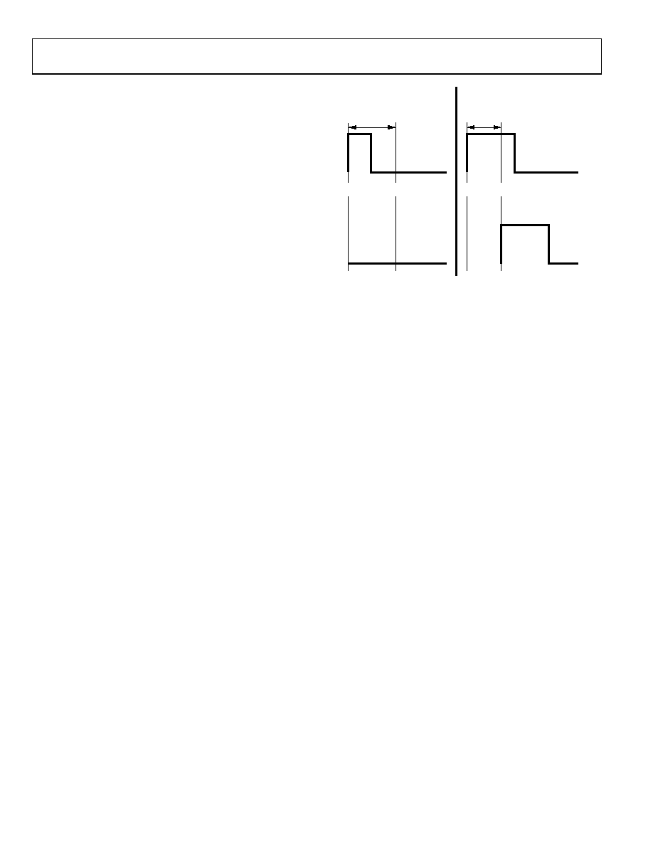
The glitch filter timeout is programmable up to 100 μs.
For example, when the glitch filter timeout is 100 μs, any pulses
appearing on the input of the glitch filter block that are less than
100 μs in duration are prevented from appearing on the output
of the glitch filter block. Any input pulse that is longer than
100 μs appears on the output of the glitch filter block. The
output is delayed with respect to the input by 100 μs. The
filtering process is shown in Figure 22.
04735-024
T0
TGF
T0
TGF
T0
TGF
T0
TGF
INPUT
INPUT PULSE SHORTER
THAN GLITCH FILTER TIMEOUT
INPUT PULSE LONGER
THAN GLITCH FILTER TIMEOUT
OUTPUT
PROGRAMMED
TIMEOUT
PROGRAMMED
TIMEOUT
INPUT
OUTPUT
Figure 22. Input Glitch Filter Function
SUPPLY SUPERVISION WITH VXn INPUTS
The VXn inputs have two functions. They can be used as either
supply fault detectors or digital logic inputs. When selected as an
analog (SFD) input, the VXn pins have very similar functionality
to the VH and VPn pins. The major difference is that the VXn
pins have only one input range: 0.573 V to 1.375 V. Therefore,
these inputs can directly supervise only the very low supplies.
However, the input impedance of the VXn pins is high, allowing
an external resistor divide network to be connected to the pin.
Thus, any supply can be potentially divided down into the input
range of the VXn pin and be supervised. This enables the
ADM1069 to monitor other supplies such as +24 V, +48 V,
and 5 V.
An additional supply supervision function is available when the
VXn pins are selected as digital inputs. In this case, the analog
function is available as a second detector on each of the dedi-
cated analog inputs, VPn and VH. The analog function of VX1
is mapped to VP1, VX2 is mapped to VP2, and so on. VX4 is
mapped to VH. In this case, these SFDs can be viewed as a
secondary or warning SFD.
The secondary SFDs are fixed to the same input range as the
primary SFD. They are used to indicate warning levels rather
than failure levels. This allows faults and warnings to be gener-
ated on a single supply using only one pin. For example, if VP1
is set to output a fault if a 3.3 V supply drops to 3.0 V, VX1 can
be set to output a warning at 3.1 V. Warning outputs are available
for readback from the status registers. They are also OR’ed
together and fed into the sequencing engine (SE), allowing
warnings to generate interrupts on the PDOs. Therefore, in this
example, if the supply drops to 3.1 V, a warning is generated,
and remedial action can be taken before the supply drops out of
tolerance.
相关PDF资料 |
PDF描述 |
|---|---|
| AFL27005DX/CHPBF | 2-OUTPUT 66 W DC-DC REG PWR SUPPLY MODULE |
| AFL27012DX/CHPBF | 2-OUTPUT 66 W DC-DC REG PWR SUPPLY MODULE |
| APE2902Y5-46 | SWITCHING REGULATOR, PDSO5 |
| APE2902Y5R-49 | SWITCHING REGULATOR, PDSO5 |
| ATW2805S/-SLV | 1-OUTPUT 30 W DC-DC REG PWR SUPPLY MODULE |
相关代理商/技术参数 |
参数描述 |
|---|---|
| ADM1069ASTZ | 功能描述:IC SUPERVISOR/SEQUENCER 32-LQFP RoHS:是 类别:集成电路 (IC) >> PMIC - 监控器 系列:Super Sequencer® 其它有关文件:STM6905 View All Specifications 标准包装:1 系列:- 类型:多压监控器 监视电压数目:5 输出:开路漏极或开路集电极 复位:低有效 复位超时:最小为 140 ms 电压 - 阀值:2.188V,2.955V,可调,可调,可调 工作温度:-40°C ~ 85°C 安装类型:表面贴装 封装/外壳:8-TSSOP,8-MSOP(0.118",3.00mm 宽) 供应商设备封装:8-TSSOP 包装:Digi-Reel® 产品目录页面:1197 (CN2011-ZH PDF) 其它名称:497-8728-6 |
| ADM1069ASTZ-REEL | 功能描述:IC SEQUENCER/SUPERVISOR 32LQFP RoHS:是 类别:集成电路 (IC) >> PMIC - 监控器 系列:Super Sequencer® 标准包装:1 系列:- 类型:简单复位/加电复位 监视电压数目:1 输出:开路漏极或开路集电极 复位:高有效 复位超时:- 电压 - 阀值:1.8V 工作温度:-40°C ~ 125°C 安装类型:表面贴装 封装/外壳:6-TSOP(0.059",1.50mm 宽)5 引线 供应商设备封装:5-TSOP 包装:剪切带 (CT) 其它名称:NCP301HSN18T1GOSCT |
| ADM1069ASTZ-REEL7 | 功能描述:IC SEQUENCER/SUPERVISOR 32LQFP RoHS:是 类别:集成电路 (IC) >> PMIC - 监控器 系列:Super Sequencer® 其它有关文件:STM6905 View All Specifications 标准包装:1 系列:- 类型:多压监控器 监视电压数目:5 输出:开路漏极或开路集电极 复位:低有效 复位超时:最小为 140 ms 电压 - 阀值:2.188V,2.955V,可调,可调,可调 工作温度:-40°C ~ 85°C 安装类型:表面贴装 封装/外壳:8-TSSOP,8-MSOP(0.118",3.00mm 宽) 供应商设备封装:8-TSSOP 包装:Digi-Reel® 产品目录页面:1197 (CN2011-ZH PDF) 其它名称:497-8728-6 |
| ADM1070 | 制造商:AD 制造商全称:Analog Devices 功能描述:-48 V Hot Swap Controller |
| ADM1070ART | 制造商:AD 制造商全称:Analog Devices 功能描述:-48 V Hot Swap Controller |
发布紧急采购,3分钟左右您将得到回复。