- 您现在的位置:买卖IC网 > PDF目录210168 > ADM1069AST-REEL7 (ANALOG DEVICES INC) 8-CHANNEL POWER SUPPLY SUPPORT CKT, PQFP32 PDF资料下载
参数资料
| 型号: | ADM1069AST-REEL7 |
| 厂商: | ANALOG DEVICES INC |
| 元件分类: | 电源管理 |
| 英文描述: | 8-CHANNEL POWER SUPPLY SUPPORT CKT, PQFP32 |
| 封装: | MS-026-BBA, LQFP-32 |
| 文件页数: | 21/36页 |
| 文件大小: | 763K |
| 代理商: | ADM1069AST-REEL7 |
第1页第2页第3页第4页第5页第6页第7页第8页第9页第10页第11页第12页第13页第14页第15页第16页第17页第18页第19页第20页当前第21页第22页第23页第24页第25页第26页第27页第28页第29页第30页第31页第32页第33页第34页第35页第36页
ADM1069
Rev. A | Page 28 of 36
SERIAL BUS INTERFACE
The ADM1069 is controlled via the serial system management
bus (SMBus) and is connected to this bus as a slave device,
under the control of a master device. It takes approximately
1 ms after power-up for the ADM1069 to download from its
EEPROM. Therefore, access to the ADM1069 is restricted until
the download is completed.
Identifying the ADM1069 on the SMBus
The ADM1069 has a 7-bit serial bus slave address (see Table 11).
The device is powered up with a default serial bus address. The
5 MSBs of the address are set to 10011; the 2 LSBs are
determined by the logical states of Pin A1 and Pin A0. This
allows the connection of four ADM1069s to one SMBus.
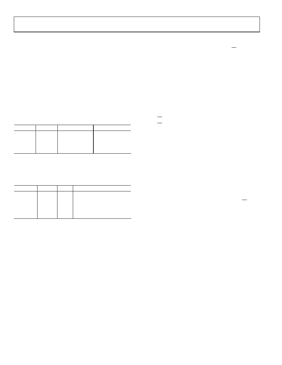
Table 11. Serial Bus Slave Address
A0 Pin
A1 Pin
Hex Address
7-Bit Address
Low
0x98
1001100X1
Low
High
0x9A
1001101X1
High
Low
0x9C
1001110X1
High
0x9E
1001111X1
1 X = Read/Write bit. The address is shown only as the first 7 MSBs.
The device also has several identification registers (read-only)
that can be read across the SMBus. Table 12 lists these registers
with their values and functions.
Table 12. Identification Register Values and Functions
Name
Address
Value
Function
MANID
0xF4
0x41
Manufacturer ID for Analog
Devices
REVID
0xF5
0x02
Silicon revision
MARK1
0xF6
0x00
Software brand
MARK2
0xF7
0x00
Software brand
General SMBus Timing
general read and write operations using the SMBus. The SMBus
specification defines specific conditions for different types of
read and write operations, which are discussed in the Write
Operations and Read Operations sections.
The general SMBus protocol operates as follows:
1.
The master initiates data transfer by establishing a start
condition, defined as a high-to-low transition on the serial
data-line SDA, while the serial clock line SCL remains
high. This indicates that a data stream follows.
All slave peripherals connected to the serial bus respond to
the start condition and shift in the next eight bits, consisting
of a 7-bit slave address (MSB first) plus an R/W bit. This
bit determines the direction of the data transfer, that is,
whether data is written to or read from the slave device
(0 = write, 1 = read).
The peripheral whose address corresponds to the transmit-
ted address responds by pulling the data line low during
the low period before the ninth clock pulse, known as the
acknowledge bit, and by holding it low during the high
period of this clock pulse.
All other devices on the bus remain idle while the selected
device waits for data to be read from or written to it. If the
R/W bit is a 0, the master writes to the slave device. If the
R/W bit is a 1, the master reads from the slave device.
2.
Data is sent over the serial bus in sequences of nine clock
pulses, eight bits of data followed by an acknowledge bit
from the slave device. Data transitions on the data line
must occur during the low period of the clock signal and
remain stable during the high period, because a low-to-
high transition when the clock is high could be interpreted
as a stop signal. If the operation is a write operation, the
first data byte after the slave address is a command byte.
This tells the slave device what to expect next. It could be
an instruction telling the slave device to expect a block
write, or it could simply be a register address that tells the
slave where subsequent data is to be written. Because data
can flow in only one direction, as defined by the R/W bit,
sending a command to a slave device during a read
operation is not possible. Before a read operation, it could
be necessary to perform a write operation to tell the slave
what sort of read operation to expect and/or the address
from which data is to be read.
3.
When all data bytes have been read or written, stop condi-
tions are established. In write mode, the master pulls the
data line high during the 10th clock pulse to assert a stop
condition. In read mode, the master device releases the
SDA line during the low period before the ninth clock
pulse, but the slave device does not pull it low. This is known
as no acknowledge. The master then takes the data line low
during the low period before the 10th clock pulse, and then
high during the 10th clock pulse to assert a stop condition.
相关PDF资料 |
PDF描述 |
|---|---|
| AFL27005DX/CHPBF | 2-OUTPUT 66 W DC-DC REG PWR SUPPLY MODULE |
| AFL27012DX/CHPBF | 2-OUTPUT 66 W DC-DC REG PWR SUPPLY MODULE |
| APE2902Y5-46 | SWITCHING REGULATOR, PDSO5 |
| APE2902Y5R-49 | SWITCHING REGULATOR, PDSO5 |
| ATW2805S/-SLV | 1-OUTPUT 30 W DC-DC REG PWR SUPPLY MODULE |
相关代理商/技术参数 |
参数描述 |
|---|---|
| ADM1069ASTZ | 功能描述:IC SUPERVISOR/SEQUENCER 32-LQFP RoHS:是 类别:集成电路 (IC) >> PMIC - 监控器 系列:Super Sequencer® 其它有关文件:STM6905 View All Specifications 标准包装:1 系列:- 类型:多压监控器 监视电压数目:5 输出:开路漏极或开路集电极 复位:低有效 复位超时:最小为 140 ms 电压 - 阀值:2.188V,2.955V,可调,可调,可调 工作温度:-40°C ~ 85°C 安装类型:表面贴装 封装/外壳:8-TSSOP,8-MSOP(0.118",3.00mm 宽) 供应商设备封装:8-TSSOP 包装:Digi-Reel® 产品目录页面:1197 (CN2011-ZH PDF) 其它名称:497-8728-6 |
| ADM1069ASTZ-REEL | 功能描述:IC SEQUENCER/SUPERVISOR 32LQFP RoHS:是 类别:集成电路 (IC) >> PMIC - 监控器 系列:Super Sequencer® 标准包装:1 系列:- 类型:简单复位/加电复位 监视电压数目:1 输出:开路漏极或开路集电极 复位:高有效 复位超时:- 电压 - 阀值:1.8V 工作温度:-40°C ~ 125°C 安装类型:表面贴装 封装/外壳:6-TSOP(0.059",1.50mm 宽)5 引线 供应商设备封装:5-TSOP 包装:剪切带 (CT) 其它名称:NCP301HSN18T1GOSCT |
| ADM1069ASTZ-REEL7 | 功能描述:IC SEQUENCER/SUPERVISOR 32LQFP RoHS:是 类别:集成电路 (IC) >> PMIC - 监控器 系列:Super Sequencer® 其它有关文件:STM6905 View All Specifications 标准包装:1 系列:- 类型:多压监控器 监视电压数目:5 输出:开路漏极或开路集电极 复位:低有效 复位超时:最小为 140 ms 电压 - 阀值:2.188V,2.955V,可调,可调,可调 工作温度:-40°C ~ 85°C 安装类型:表面贴装 封装/外壳:8-TSSOP,8-MSOP(0.118",3.00mm 宽) 供应商设备封装:8-TSSOP 包装:Digi-Reel® 产品目录页面:1197 (CN2011-ZH PDF) 其它名称:497-8728-6 |
| ADM1070 | 制造商:AD 制造商全称:Analog Devices 功能描述:-48 V Hot Swap Controller |
| ADM1070ART | 制造商:AD 制造商全称:Analog Devices 功能描述:-48 V Hot Swap Controller |
发布紧急采购,3分钟左右您将得到回复。