- 您现在的位置:买卖IC网 > PDF目录16832 > ADM1169ACPZ (Analog Devices Inc)IC SEQUENCER/SUPERVISOR 40LFCSP PDF资料下载
参数资料
| 型号: | ADM1169ACPZ |
| 厂商: | Analog Devices Inc |
| 文件页数: | 17/36页 |
| 文件大小: | 0K |
| 描述: | IC SEQUENCER/SUPERVISOR 40LFCSP |
| 标准包装: | 1 |
| 系列: | Super Sequencer® |
| 应用: | 电源监控器,序列发生器 |
| 输入电压: | 3 V ~ 14.4 V |
| 电源电压: | 3 V ~ 14.4 V |
| 电流 - 电源: | 4.2mA |
| 工作温度: | -40°C ~ 85°C |
| 安装类型: | 表面贴装 |
| 封装/外壳: | 40-WFQFN 裸露焊盘,CSP |
| 供应商设备封装: | 40-LFCSP-WQ(6x6) |
| 包装: | 托盘 |
第1页第2页第3页第4页第5页第6页第7页第8页第9页第10页第11页第12页第13页第14页第15页第16页当前第17页第18页第19页第20页第21页第22页第23页第24页第25页第26页第27页第28页第29页第30页第31页第32页第33页第34页第35页第36页
�� ��
��
��Data� Sheet�
�OUTPUTS�
�SUPPLY� SEQUENCING� THROUGH� CONFIGURABLE�
�OUTPUT� DRIVERS�
�Supply� sequencing� is� achieved� with� the� ADM1169� using� the�
�programmable� driver� outputs� (PDOs)� on� the� device� as� control�
�signals� for� supplies.� The� output� drivers� can� be� used� as� logic�
�enables� or� as� FET� drivers.�
�The� sequence� in� which� the� PDOs� are� asserted� (and,� therefore,�
�the� supplies� are� turned� on)� is� controlled� by� the� SE.� The� SE�
�determines� what� action� is� taken� with� the� PDOs� based� on� the�
�condition� of� the� ADM1169� inputs.� Therefore,� the� PDOs� can� be�
�set� up� to� assert� when� the� SFDs� are� in� tolerance,� the� correct� input�
�signals� are� received� on� the� VXx� digital� pins,� and� no� warnings�
�are� received� from� any� of� the� inputs� of� the� devices.� The� PDOs�
�can� be� used� for� a� variety� of� functions.� The� primary� function� is�
�to� provide� enable� signals� for� LDOs� or� dc-to-dc� converters� that�
�generate� supplies� locally� on� a� board.� The� PDOs� can� also� be� used�
�to� provide� a� PWRGD� signal� when� all� the� SFDs� are� in� tolerance�
�or� a� RESET� output� if� one� of� the� SFDs� goes� out� of� specification�
�(this� can� be� used� as� a� status� signal� for� a� DSP,� FPGA,� or� other�
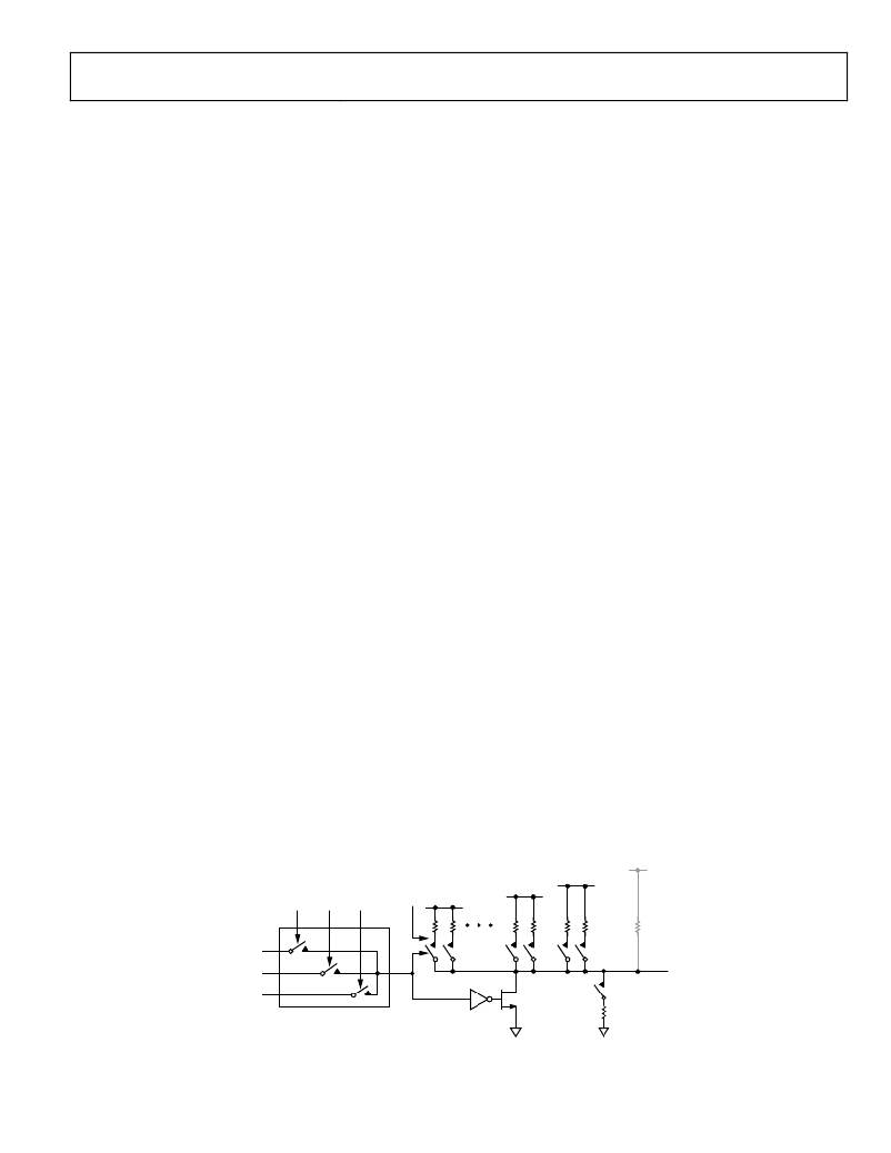
�ADM1169�
�The� data� driving� each� of� the� PDOs� can� come� from� one� of� three�
�sources.� The� source� can� be� enabled� in� the� PDOxCFG� configuration�
�register� (see� the� AN-721� Application� Note� for� details).�
�The� data� sources� are� as� follows:�
�?� Output� from� the� SE.�
�?� Directly� from� the� SMBus.� A� PDO� can� be� configured� so� that�
�the� SMBus� has� direct� control� over� it.� This� enables� software�
�control� of� the� PDOs.� Therefore,� a� microcontroller� can� be�
�used� to� initiate� a� software� power-up/power-down� sequence.�
�?� On-chip� clock.� A� 100� kHz� clock� is� generated� on� the� device.�
�This� clock� can� be� made� available� on� any� of� the� PDOs.� It� can� be�
�used,� for� example,� to� clock� an� external� device� such� as� an� LED.�
�DEFAULT� OUTPUT� CONFIGURATION�
�All� of� the� internal� registers� in� an� unprogrammed� ADM1169� device�
�from� the� factory� are� set� to� 0.� Because� of� this,� the� PDOx� pins� are�
�pulled� to� GND� by� a� weak� (20� k?),� on-chip,� pull-down� resistor.�
�As� the� input� supply� to� the� ADM1169� ramps� up� on� VPx� or� VH,�
�all� PDOx� pins� behave� as� follows:�
�microcontroller).�
�The� PDOs� can� be� programmed� to� pull� up� to� a� number� of� different�
�options.� The� outputs� can� be� programmed� as� follows:�
�?�
�?�
�Input� supply� =� 0� V� to� 1.2� V.� The� PDOs� are� high� impedance.�
�Input� supply� =� 1.2� V� to� 2.7� V.� The� PDOs� are� pulled� to� GND�
�by� a� weak� (20� k?),� on-chip,� pull-down� resistor.�
�?�
�?�
�?�
�?�
�?�
�?�
�?�
�Open-drain� (allowing� the� user� to� connect� an� external� pull-up�
�resistor)�
�Open-drain� with� weak� pull-up� to� V� DD�
�Open-drain� with� strong� pull-up� to� V� DD�
�Open-drain� with� weak� pull-up� to� VPx�
�Open-drain� with� strong� pull-up� to� VPx.�
�Strong� pull-down� to� GND�
�Internally� charge-pumped� high� drive� (12� V,� PDO1� to�
�PDO6� only)�
�?� Supply� >� 2.7� V.� Factory� programmed� devices� continue� to�
�pull� all� PDOs� to� GND� by� a� weak� (20� k?),� on-chip,� pull-down�
�resistor.� Programmed� devices� download� current� EEPROM�
�configuration� data,� and� the� programmed� setup� is� latched.� The�
�PDO� then� goes� to� the� state� demanded� by� the� configuration.�
�This� provides� a� known� condition� for� the� PDOs� during�
�power-up.�
�The� internal� pull-down� can� be� overdriven� with� an� external� pull-up�
�of� suitable� value� tied� from� the� PDOx� pin� to� the� required� pull-up�
�voltage.� The� 20� k?� resistor� must� be� accounted� for� in� calculating�
�The� last� option� (available� only� on� PDO1� to� PDO6)� allows� the�
�user� to� directly� drive� a� voltage� high� enough� to� fully� enhance� an�
�external� NFET,� which� is� used� to� isolate,� for� example,� a� card-side�
�voltage� from� a� backplane� supply� (a� PDO� can� sustain� greater� than�
�10.5� V� into� a� 1� μA� load).� The� pull-down� switches� can� also� be�
�used� to� drive� status� LEDs� directly.�
�a� suitable� value.� For� example,� if� PDOx� must� be� pulled� up� to� 3.3� V,�
�and� 5� V� is� available� as� an� external� supply,� the� pull-up� resistor�
�value� is� given� by�
�3.3� V� =� 5� V� � 20� k?/(� R� UP� +� 20� k?)�
�Therefore,�
�R� UP� =� (100� k?� ?� 66� k?)/3.3� V� =� 10� k?�
�VFET� (PDO1� TO� PDO6� ONLY)�
�V� DD�
�VP4�
�SE� DATA�
�SMBus� DATA�
�CFG4� CFG5� CFG6�
�SEL�
�VP1�
�PDO�
�CLK� DATA�
�Figure� 25.� Programmable� Driver� Output�
�Rev.� A� |� Page� 17� of� 36�
�相关PDF资料 |
PDF描述 |
|---|---|
| SFSD-20-28-H-05.00-DR-NDX | CABLE ASSY SOCKET 40POS 28AWG |
| 207W234-25-01-0 | BOOT MOLDED |
| 382W042-25-0 | BOOT MOLDED |
| 382W042-3-0 | BOOT MOLDED |
| IS-DEV KIT-7D | KIT DEV FOR OLED DISPLAY |
相关代理商/技术参数 |
参数描述 |
|---|---|
| ADM1169ACPZ-RL7 | 功能描述:IC SEQUENCER/SUPERVISOR 40LFCSP RoHS:是 类别:集成电路 (IC) >> PMIC - 电源控制器,监视器 系列:Super Sequencer® 产品培训模块:Lead (SnPb) Finish for COTS Obsolescence Mitigation Program 标准包装:2,500 系列:- 应用:多相控制器 输入电压:- 电源电压:9 V ~ 14 V 电流 - 电源:- 工作温度:-40°C ~ 85°C 安装类型:表面贴装 封装/外壳:40-WFQFN 裸露焊盘 供应商设备封装:40-TQFN-EP(5x5) 包装:带卷 (TR) |
| ADM1169ARTZ | 制造商:Analog Devices 功能描述:SUPER SEQUENCER W/ BLACK BOX - Tape and Reel |
| ADM1169ASTZ | 功能描述:IC SEQUENCER/SUPERVISOR 32LQFP RoHS:是 类别:集成电路 (IC) >> PMIC - 电源控制器,监视器 系列:Super Sequencer® 产品培训模块:Lead (SnPb) Finish for COTS Obsolescence Mitigation Program 标准包装:2,500 系列:- 应用:多相控制器 输入电压:- 电源电压:9 V ~ 14 V 电流 - 电源:- 工作温度:-40°C ~ 85°C 安装类型:表面贴装 封装/外壳:40-WFQFN 裸露焊盘 供应商设备封装:40-TQFN-EP(5x5) 包装:带卷 (TR) |
| ADM1169ASTZ-RL7 | 功能描述:IC SEQUENCER/SUPERVISOR 32LQFP RoHS:是 类别:集成电路 (IC) >> PMIC - 电源控制器,监视器 系列:Super Sequencer® 产品培训模块:Lead (SnPb) Finish for COTS Obsolescence Mitigation Program 标准包装:2,500 系列:- 应用:多相控制器 输入电压:- 电源电压:9 V ~ 14 V 电流 - 电源:- 工作温度:-40°C ~ 85°C 安装类型:表面贴装 封装/外壳:40-WFQFN 裸露焊盘 供应商设备封装:40-TQFN-EP(5x5) 包装:带卷 (TR) |
| ADM1170 | 制造商:AD 制造商全称:Analog Devices 功能描述:1.6 V to 16.5 V Hot Swap Controller with Soft Start |
发布紧急采购,3分钟左右您将得到回复。