- 您现在的位置:买卖IC网 > PDF目录9663 > ADN2804ACPZ-RL7 (Analog Devices Inc)IC CLK/DATA REC 622MBPS 32-LFCSP PDF资料下载
参数资料
| 型号: | ADN2804ACPZ-RL7 |
| 厂商: | Analog Devices Inc |
| 文件页数: | 15/24页 |
| 文件大小: | 0K |
| 描述: | IC CLK/DATA REC 622MBPS 32-LFCSP |
| 标准包装: | 1,500 |
| 类型: | 时钟和数据恢复(CDR),多路复用器 |
| PLL: | 是 |
| 主要目的: | SONET/SDH |
| 输入: | CML |
| 输出: | LVDS |
| 电路数: | 1 |
| 比率 - 输入:输出: | 1:2 |
| 差分 - 输入:输出: | 是/是 |
| 频率 - 最大: | 622MHz |
| 电源电压: | 3 V ~ 3.6 V |
| 工作温度: | -40°C ~ 85°C |
| 安装类型: | 表面贴装 |
| 封装/外壳: | 32-VFQFN 裸露焊盘,CSP |
| 供应商设备封装: | 32-LFCSP-VQ(5x5) |
| 包装: | 带卷 (TR) |
ADN2804
Data Sheet
Rev. C | Page 22 of 24
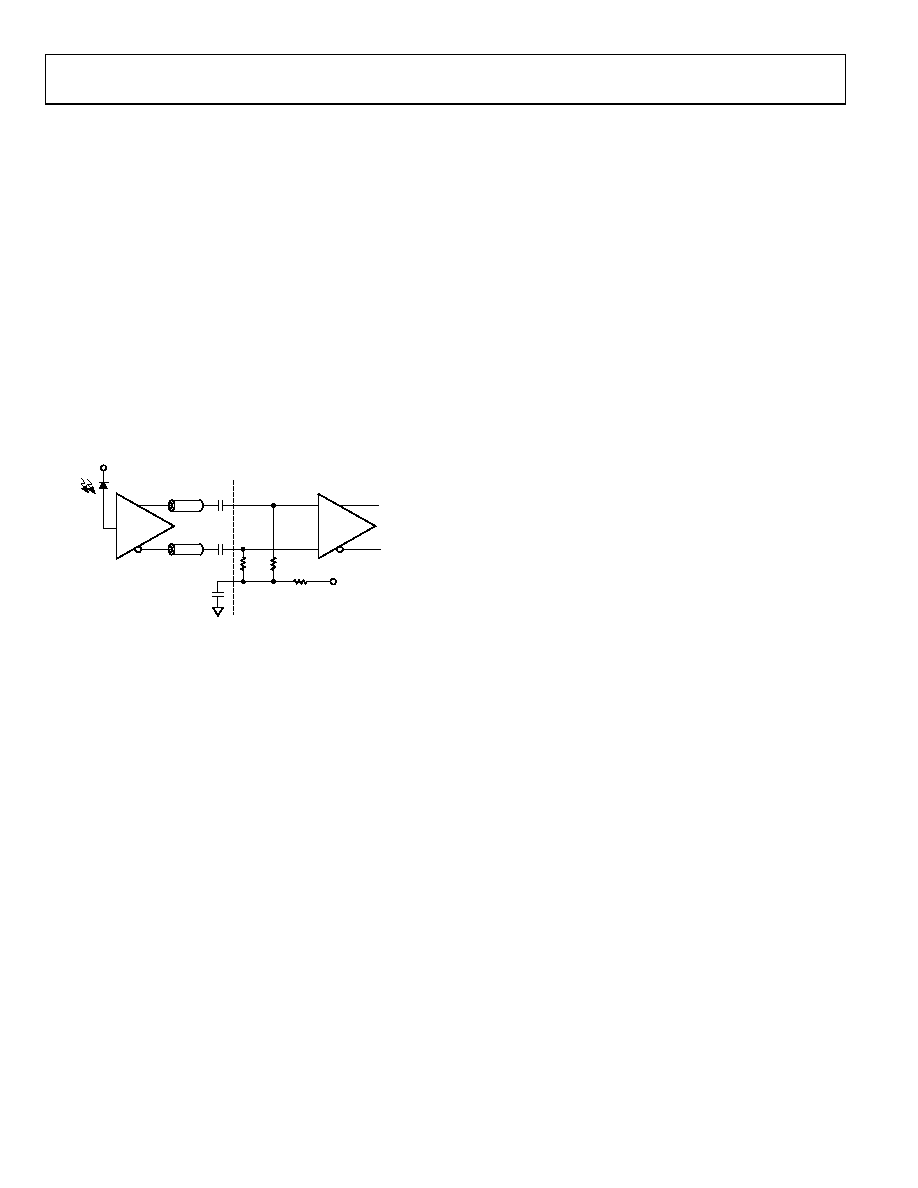
Transmission Lines
Minimizing reflections in the ADN2804 requires use of 50 Ω
transmission lines for all pins with high frequency input and
output signals, including PIN, NIN, CLKOUTP, CLKOUTN,
DATAOUTP, and DATAOUTN (also REFCLKP and REFCLKN,
if a high frequency reference clock is used, such as 155 MHz). It
is also necessary for the PIN/NIN input traces to be matched in
length and for the CLKOUTP/CLKOUTN and
DATAOUTP/DATAOUTN output traces to be matched in
length to avoid skew between the differential traces.
The high speed inputs, PIN and NIN, are internally terminated
with 50 Ω to an internal reference voltage (see Figure 25).
A 0.1 μF is recommended between VREF, Pin 3, and GND to
provide an ac ground for the inputs.
As with any high speed, mixed-signal design, take care to keep
all high speed digital traces away from sensitive analog nodes.
CIN
0.1F
NIN
PIN
ADN2804
2.5V
VREF
TIA
VCC
0
58
01
-0
26
50
3
Figure 25. ADN2804 AC-Coupled Input Configuration
Soldering Guidelines for Lead Frame Chip Scale Package
The lands on the 32-lead LFCSP are rectangular. The printed
circuit board (PCB) pad for these should be 0.1 mm longer than
the package land length and 0.05 mm wider than the package
land width. The land should be centered on the pad. This
ensures that the solder joint size is maximized. The bottom of
the chip scale package has a central exposed pad. The pad on
the PCB should be at least as large as this exposed pad. The user
must connect the exposed pad to VEE using plugged vias so
that solder does not leak through the vias during reflow. This
ensures a solid connection from the exposed pad to VEE.
Choosing AC Coupling Capacitors
AC coupling capacitors at the input (PIN, NIN) and output
(DATAOUTP, DATAOUTN) of the ADN2804 can be optimized
for the application. When choosing the capacitors, the time
constant formed with the two 50 Ω resistors in the signal path
must be considered. When a large number of consecutive
identical digits (CIDs) are applied, the capacitor voltage can
droop due to baseline wander (see Figure 26), causing pattern-
dependent jitter (PDJ).
The user must determine how much droop is tolerable and
choose an ac coupling capacitor based on that amount of droop.
The amount of PDJ can then be approximated based on the
capacitor selection. The actual capacitor value selection can
require some trade-offs between droop and PDJ.
For example, assuming that 2% droop can be tolerated, the
maximum differential droop is 4%. Normalizing to V p-p:
Droop = ΔV = 0.04 V = 0.5 V p-p (1 et/τ); therefore, τ = 12t
where:
τ is the RC time constant (C is the ac coupling capacitor, R =
100 Ω seen by C).
t is the total discharge time, which is equal to nT, where n is the
number of CIDs, and T is the bit period.
The capacitor value can then be calculated by combining the
equations for τ and t:
C = 12 nT/R
Once the capacitor value is selected, the PDJ can be
approximated as
PDJpspp = 0.5 tr(1 e(nT/RC))/0.6
where:
PDJpspp is the amount of pattern-dependent jitter allowed
(<0.01 UI p-p typical).
tr is the rise time, which is equal to 0.22/BW,
where BW ~ 0.7 (bit rate).
Note that this expression for tr is accurate only for the inputs.
The output rise time for the ADN2804 is ~100 ps regardless of
the data rate.
相关PDF资料 |
PDF描述 |
|---|---|
| MS3120F22-55P | CONN RCPT 55POS WALL MNT W/PINS |
| MS27497E24B2PA | CONN RCPT 100POS WALL MNT W/PINS |
| AD9523BCPZ-REEL7 | IC INTEGER-N CLCK GEN 72LFCSP |
| PT06A-20-16P | CONN PLUG 16 POS STRAIGHT W/PINS |
| VE-JTW-MX-F3 | CONVERTER MOD DC/DC 5.5V 75W |
相关代理商/技术参数 |
参数描述 |
|---|---|
| ADN2805 | 制造商:AD 制造商全称:Analog Devices 功能描述:1.25 Gbps Clock and Data Recovery IC |
| ADN2805ACPZ | 功能描述:IC CLK/DATA REC 1.25GBPS 32LFCSP RoHS:是 类别:集成电路 (IC) >> 时钟/计时 - 专用 系列:- 标准包装:1 系列:- 类型:时钟/频率发生器,多路复用器 PLL:是 主要目的:存储器,RDRAM 输入:晶体 输出:LVCMOS 电路数:1 比率 - 输入:输出:1:2 差分 - 输入:输出:无/是 频率 - 最大:400MHz 电源电压:3 V ~ 3.6 V 工作温度:0°C ~ 85°C 安装类型:表面贴装 封装/外壳:16-TSSOP(0.173",4.40mm 宽) 供应商设备封装:16-TSSOP 包装:Digi-Reel® 其它名称:296-6719-6 |
| ADN2805ACPZ-500RL7 | 功能描述:IC CLK/DATA REC 1.25GBPS 32LFCSP RoHS:是 类别:集成电路 (IC) >> 时钟/计时 - 专用 系列:- 标准包装:28 系列:- 类型:时钟/频率发生器 PLL:是 主要目的:Intel CPU 服务器 输入:时钟 输出:LVCMOS 电路数:1 比率 - 输入:输出:3:22 差分 - 输入:输出:无/是 频率 - 最大:400MHz 电源电压:3.135 V ~ 3.465 V 工作温度:0°C ~ 85°C 安装类型:表面贴装 封装/外壳:64-TFSOP (0.240",6.10mm 宽) 供应商设备封装:64-TSSOP 包装:管件 |
| ADN2805ACPZ-RL7 | 功能描述:IC CLK/DATA REC 1.25GBPS 32LFCSP RoHS:是 类别:集成电路 (IC) >> 时钟/计时 - 专用 系列:- 标准包装:28 系列:- 类型:时钟/频率发生器 PLL:是 主要目的:Intel CPU 服务器 输入:时钟 输出:LVCMOS 电路数:1 比率 - 输入:输出:3:22 差分 - 输入:输出:无/是 频率 - 最大:400MHz 电源电压:3.135 V ~ 3.465 V 工作温度:0°C ~ 85°C 安装类型:表面贴装 封装/外壳:64-TFSOP (0.240",6.10mm 宽) 供应商设备封装:64-TSSOP 包装:管件 |
| ADN2806 | 制造商:AD 制造商全称:Analog Devices 功能描述:622 Mbps Clock and Data Recovery IC |
发布紧急采购,3分钟左右您将得到回复。