- 您现在的位置:买卖IC网 > PDF目录9663 > ADN2804ACPZ-RL7 (Analog Devices Inc)IC CLK/DATA REC 622MBPS 32-LFCSP PDF资料下载
参数资料
| 型号: | ADN2804ACPZ-RL7 |
| 厂商: | Analog Devices Inc |
| 文件页数: | 8/24页 |
| 文件大小: | 0K |
| 描述: | IC CLK/DATA REC 622MBPS 32-LFCSP |
| 标准包装: | 1,500 |
| 类型: | 时钟和数据恢复(CDR),多路复用器 |
| PLL: | 是 |
| 主要目的: | SONET/SDH |
| 输入: | CML |
| 输出: | LVDS |
| 电路数: | 1 |
| 比率 - 输入:输出: | 1:2 |
| 差分 - 输入:输出: | 是/是 |
| 频率 - 最大: | 622MHz |
| 电源电压: | 3 V ~ 3.6 V |
| 工作温度: | -40°C ~ 85°C |
| 安装类型: | 表面贴装 |
| 封装/外壳: | 32-VFQFN 裸露焊盘,CSP |
| 供应商设备封装: | 32-LFCSP-VQ(5x5) |
| 包装: | 带卷 (TR) |
ADN2804
Data Sheet
Rev. C | Page 16 of 24
FUNCTIONAL DESCRIPTION
FREQUENCY ACQUISITION
The ADN2804 acquires frequency from the data. The lock
detector circuit compares the frequency of the VCO and the
frequency of the incoming data. When these frequencies differ
by more than 1000 ppm, LOL is asserted. This initiates a frequency
acquisition cycle. When the VCO frequency is within 250 ppm
of the data frequency, LOL is deasserted.
Once LOL is deasserted, the frequency-locked loop is turned
off. The PLL/DLL pulls the VCO frequency in the rest of the
way until the VCO frequency equals the data frequency.
The frequency loop requires a single external capacitor between
CF1 and CF2, Pin 14 and Pin 15. A 0.47 μF ± 20%, X7R ceramic
chip capacitor with <10 nA leakage current is recommended.
Leakage current of the capacitor can be calculated by dividing
the maximum voltage across the 0.47 μF capacitor, ~3 V, by the
insulation resistance of the capacitor. The insulation resistance
of the 0.47 μF capacitor should be greater than 300 MΩ.
LIMITING AMPLIFIER
The limiting amplifier has differential inputs (PIN/NIN) that
are internally terminated with 50 Ω to an on-chip voltage
reference (VREF = 2.5 V typically). The inputs are typically
ac-coupled externally, although dc coupling is possible as long
as the input common-mode voltage remains above 2.5 V (see
Input offset is factory trimmed to achieve better than 3.3 mV
typical sensitivity with minimal drift. The limiting amplifier can
be driven differentially or in a single-ended fashion.
SLICE ADJUST
The quantizer slicing level can be offset by ±100 mV to mitigate
the effect of amplified spontaneous emission (ASE) noise or duty
cycle distortion by applying a differential voltage input of up to
±0.95 V to the SLICEP and SLICEN inputs. If no adjustment of
the slice level is needed, SLICEP and SLICEN should be tied to
VEE. The gain of the slice adjustment is ~0.11 V/V.
LOSS-OF-SIGNAL (LOS) DETECTOR
The receiver front-end LOS detector circuit detects when the
input signal level falls below a user-adjustable threshold. The
threshold is set with a single external resistor from Pin 9,
THRADJ, to VEE. The LOS comparator trip point vs. the
resistor value is shown in Figure 6. If the input level to the
ADN2804 drops below the programmed LOS threshold, the
output of the LOS detector, LOS (Pin 22), is asserted to Logic 1.
The LOS detector’s response time is ~500 ns by design, but is
dominated by the RC time constant in ac-coupled applications.
The LOS pin defaults to active high. However, setting Bit
CTRLC[2] to 1, configures the LOS pin as active low.
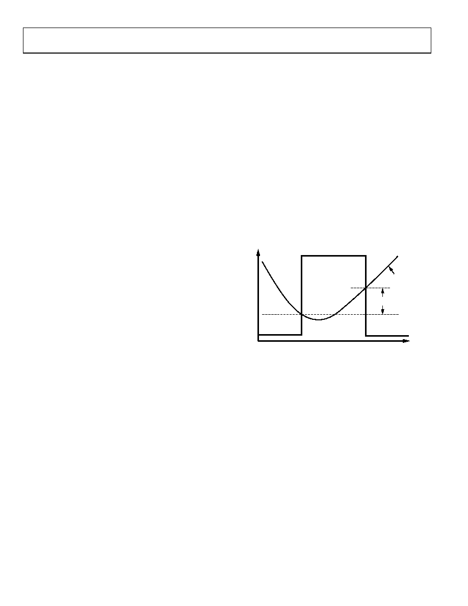
There is typically 6 dB of electrical hysteresis designed into the
LOS detector to prevent chatter on the LOS pin. If the input
level drops below the programmed LOS threshold causing the
LOS pin to assert, the LOS pin deasserts after the input level
increases to 6 dB (2×) above the LOS threshold (see Figure 19).
HYSTERESIS
LOS OUTPUT
INPUT LEVEL
LOS THRESHOLD
t
IN
PU
T
VO
LT
A
G
E
(V
DI
F
)
0
58
01
-0
19
Figure 19. LOS Detector Hysteresis
The LOS detector and the SLICE level adjust can be used
simultaneously on the ADN2804. This means that any offset
added to the input signal by the SLICE adjust pins does not affect
the LOS detector’s measurement of the absolute input level.
相关PDF资料 |
PDF描述 |
|---|---|
| MS3120F22-55P | CONN RCPT 55POS WALL MNT W/PINS |
| MS27497E24B2PA | CONN RCPT 100POS WALL MNT W/PINS |
| AD9523BCPZ-REEL7 | IC INTEGER-N CLCK GEN 72LFCSP |
| PT06A-20-16P | CONN PLUG 16 POS STRAIGHT W/PINS |
| VE-JTW-MX-F3 | CONVERTER MOD DC/DC 5.5V 75W |
相关代理商/技术参数 |
参数描述 |
|---|---|
| ADN2805 | 制造商:AD 制造商全称:Analog Devices 功能描述:1.25 Gbps Clock and Data Recovery IC |
| ADN2805ACPZ | 功能描述:IC CLK/DATA REC 1.25GBPS 32LFCSP RoHS:是 类别:集成电路 (IC) >> 时钟/计时 - 专用 系列:- 标准包装:1 系列:- 类型:时钟/频率发生器,多路复用器 PLL:是 主要目的:存储器,RDRAM 输入:晶体 输出:LVCMOS 电路数:1 比率 - 输入:输出:1:2 差分 - 输入:输出:无/是 频率 - 最大:400MHz 电源电压:3 V ~ 3.6 V 工作温度:0°C ~ 85°C 安装类型:表面贴装 封装/外壳:16-TSSOP(0.173",4.40mm 宽) 供应商设备封装:16-TSSOP 包装:Digi-Reel® 其它名称:296-6719-6 |
| ADN2805ACPZ-500RL7 | 功能描述:IC CLK/DATA REC 1.25GBPS 32LFCSP RoHS:是 类别:集成电路 (IC) >> 时钟/计时 - 专用 系列:- 标准包装:28 系列:- 类型:时钟/频率发生器 PLL:是 主要目的:Intel CPU 服务器 输入:时钟 输出:LVCMOS 电路数:1 比率 - 输入:输出:3:22 差分 - 输入:输出:无/是 频率 - 最大:400MHz 电源电压:3.135 V ~ 3.465 V 工作温度:0°C ~ 85°C 安装类型:表面贴装 封装/外壳:64-TFSOP (0.240",6.10mm 宽) 供应商设备封装:64-TSSOP 包装:管件 |
| ADN2805ACPZ-RL7 | 功能描述:IC CLK/DATA REC 1.25GBPS 32LFCSP RoHS:是 类别:集成电路 (IC) >> 时钟/计时 - 专用 系列:- 标准包装:28 系列:- 类型:时钟/频率发生器 PLL:是 主要目的:Intel CPU 服务器 输入:时钟 输出:LVCMOS 电路数:1 比率 - 输入:输出:3:22 差分 - 输入:输出:无/是 频率 - 最大:400MHz 电源电压:3.135 V ~ 3.465 V 工作温度:0°C ~ 85°C 安装类型:表面贴装 封装/外壳:64-TFSOP (0.240",6.10mm 宽) 供应商设备封装:64-TSSOP 包装:管件 |
| ADN2806 | 制造商:AD 制造商全称:Analog Devices 功能描述:622 Mbps Clock and Data Recovery IC |
发布紧急采购,3分钟左右您将得到回复。