参数资料
| 型号: | ADN4605ABPZ |
| 厂商: | Analog Devices Inc |
| 文件页数: | 27/56页 |
| 文件大小: | 0K |
| 描述: | IC CROSSPOINT SWITCH 352BGA |
| 标准包装: | 1 |
| 系列: | XStream™ |
| 功能: | 交叉点开关 |
| 电路: | 1 x 40:40 |
| 电压电源: | 单电源 |
| 电压 - 电源,单路/双路(±): | 2.25 V ~ 3.6 V |
| 电流 - 电源: | 55mA |
| 工作温度: | -40°C ~ 85°C |
| 安装类型: | 表面贴装 |
| 封装/外壳: | 352-LBGA 裸露焊盘 |
| 供应商设备封装: | 352-BGA-EP(35x35) |
| 包装: | 托盘 |
第1页第2页第3页第4页第5页第6页第7页第8页第9页第10页第11页第12页第13页第14页第15页第16页第17页第18页第19页第20页第21页第22页第23页第24页第25页第26页当前第27页第28页第29页第30页第31页第32页第33页第34页第35页第36页第37页第38页第39页第40页第41页第42页第43页第44页第45页第46页第47页第48页第49页第50页第51页第52页第53页第54页第55页第56页
Data Sheet
ADN4605
Rev. A | Page 33 of 56
I2C SERIAL CONTROL INTERFACE
interface. To access the I2C serial interface, both the SER/PAR
line and I2C/SPI lines must be held at logic high. The ADN4605
acts only as an I2C slave device. Therefore, the I2C bus in the
system needs to include an I2C master to configure the
The ADN4605 I2C interface can be run in the standard
(100 kHz) and fast (400 kHz) modes. The SDA line only
changes value when the SCL pin is low with two exceptions.
To indicate the beginning or continuation of a transfer, the
SDA pin is driven low while the SCL pin is high; to indicate
the end of a transfer, the SDA line is driven high while the
SCL line is high. Therefore, it is important to control the
SCL clock to toggle only when the SDA line is stable unless
indicating a start, repeated start, or stop condition. To establish
(ADDR[7:1]) need to be configured to the user-assigned I2C
device address as shown in Table 17.
Table 17. Example of I2C Device Address Assignment
A7
A6
A5
A4
A3
A2
A1
A0
I2C Device Address
1
0
1
0
X
0x90
1
0
1
0
1
X
0x92
1
0
1
0
1
0
X
0x94
1
0
1
0
1
X
0x96
I2C DATA WRITE
To write data to the ADN4605 register set, a microcontroller, or
any other I2C master, must send the appropriate control signals
to the ADN4605 slave device. The steps to be followed are listed
below; the signals are controlled by the I2C master unless other-
wise specified. A diagram of the procedure is shown in Figure 46.
1. Send a start condition (while holding the SCL line high,
pull the SDA line low).
2. Send the ADN4605 part address (seven bits) whose bits are
controlled by the input pins ADDR[7:1]. This transfer
should be MSB first.
3. Send the write indicator bit (0).
4. Wait for the ADN4605 to acknowledge the request.
5. Send the register address (eight bits) to which data is to be
written. This transfer should be MSB first.
6. Wait for the ADN4605 to acknowledge the request.
7. Send the data (eight bits) to be written to the register
whose address was set in Step 5. This transfer should be
MSB first.
8. Wait for the ADN4605 to acknowledge the request.
9. Do one or more of the following:
a. Send a stop condition (while holding the SCL line high,
pull the SDA line high) and release control of the bus.
b. Send a repeated start condition (while holding the
SCL line high, pull the SDA line low) and continue
with Step 2 of the write procedure (see the I2C Data
Write section) to perform a write.
c. Send a repeated start condition (while holding the
SCL line high, pull the SDA line low) and continue
with Step 2 of this procedure to perform a read from
another address.
d. Send a repeated start condition (while holding the
SCL line high, pull the SDA line low) and continue
with Step 8 of this procedure to perform a read from
the same address.
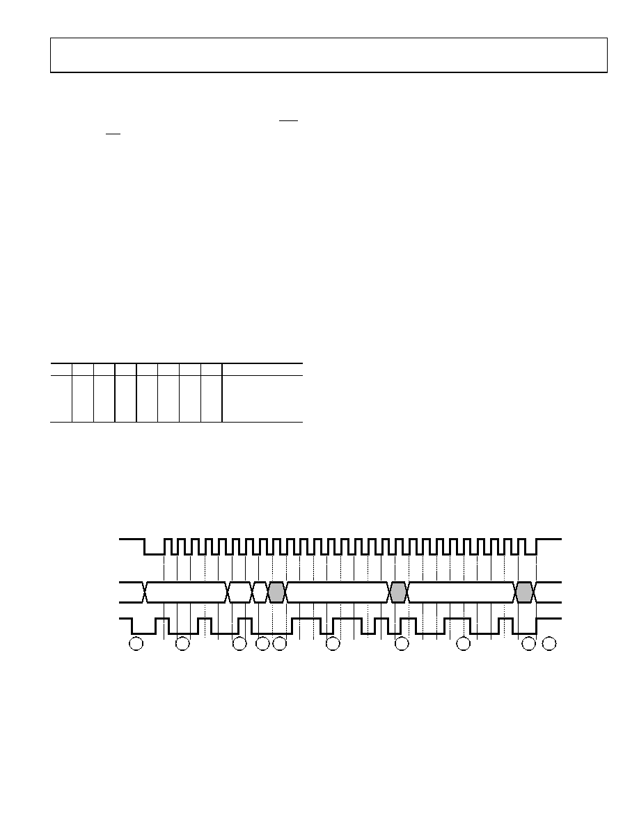
The ADN4605 write process is shown in Figure 46. The SCL
signal is shown along with a general write operation and a
specific example. In the example, Data 0x4B is written to
Address 0x6D of an ADN4605 part with a part address of 0x92.
The ADN4605 device address selections are more flexible than
shown. It is important to note that the SDA line only changes
when the SCL line is low, except for the case of sending a start,
stop, or repeated start condition, Step 1 and Step 9 in this case.
START
R/W ACK
ACK
STOP
DATA
ADDR
[1:0]
b10010
REGISTER ADDR
SCL
SDA
EXAMPLE
1
2
3
4
5
6
7
8
9a
09796-
013
Figure 46. I2C Write Diagram
相关PDF资料 |
PDF描述 |
|---|---|
| ADN4661BRZ-REEL7 | IC DRIVER DIFF LVDS 1CH 8SOIC |
| ADN4662BRZ-REEL7 | IC RCVR DIFF LVDS 1CH 8SOIC |
| ADN4663BRZ-REEL7 | IC DRIVER DIFF LVDS 2CH 8SOIC |
| ADN4664BRZ-REEL7 | IC RCVR DIFF LVDS 2CH 8SOIC |
| ADN4665ARZ-REEL7 | IC DRIVER DIFF LVDS QUAD 16SOIC |
相关代理商/技术参数 |
参数描述 |
|---|---|
| ADN4605-EVALZ | 功能描述:BOARD EVAL FOR ADN4605 RoHS:是 类别:编程器,开发系统 >> 评估演示板和套件 系列:* 标准包装:1 系列:PCI Express® (PCIe) 主要目的:接口,收发器,PCI Express 嵌入式:- 已用 IC / 零件:DS80PCI800 主要属性:- 次要属性:- 已供物品:板 |
| ADN4612 | 制造商:AD 制造商全称:Analog Devices 功能描述:11.3 Gbps 12X12 Digital Crosspoint |
| ADN4612ACPZ | 功能描述:模拟和数字交叉点 IC 12X12 Digital Crosspoint X-Grade RoHS:否 制造商:Micrel 配置:2 x 2 封装 / 箱体:MLF-16 数据速率:10.7 Gbps 输入电平:CML, LVDS, LVPECL 输出电平:CML 电源电压-最大:3.6 V 电源电压-最小:2.375 V 最大工作温度:+ 85 C 最小工作温度:- 40 C 产品:Digital Crosspoint 封装:Tube |
| ADN4650BRSZ | 功能描述:General Purpose Digital Isolator 3750Vrms 2 Channel 600Mbps 25kV/μs CMTI 20-SSOP (0.209", 5.30mm Width) 制造商:analog devices inc. 系列:iCoupler? 包装:托盘 零件状态:在售 技术:磁耦合 类型:通用 隔离式电源:无 通道数:2 输入 - 输入侧 1/输入侧 2:2/0 通道类型:单向 电压 - 隔离:3750Vrms 共模瞬态抗扰度(最小值):25kV/μs 数据速率:600Mbps 传播延迟 tpLH / tpHL(最大值):4.5ns,4.5ns 脉宽失真(最大):- 上升/下降时间(典型值):350ps,350ps(最大) 电压 - 电源:2.375 V ~ 2.625 V 工作温度:-40°C ~ 125°C 封装/外壳:20-SSOP(0.209",5.30mm 宽) 供应商器件封装:20-SSOP 标准包装:66 |
| ADN4650BRSZ-RL7 | 功能描述:General Purpose Digital Isolator 3750Vrms 2 Channel 600Mbps 25kV/μs CMTI 20-SSOP (0.209", 5.30mm Width) 制造商:analog devices inc. 系列:iCoupler? 包装:剪切带(CT) 零件状态:在售 技术:磁耦合 类型:通用 隔离式电源:无 通道数:2 输入 - 输入侧 1/输入侧 2:2/0 通道类型:单向 电压 - 隔离:3750Vrms 共模瞬态抗扰度(最小值):25kV/μs 数据速率:600Mbps 传播延迟 tpLH / tpHL(最大值):4.5ns,4.5ns 脉宽失真(最大):- 上升/下降时间(典型值):350ps,350ps(最大) 电压 - 电源:2.375 V ~ 2.625 V 工作温度:-40°C ~ 125°C 封装/外壳:20-SSOP(0.209",5.30mm 宽) 供应商器件封装:20-SSOP 标准包装:1 |
发布紧急采购,3分钟左右您将得到回复。