- 您现在的位置:买卖IC网 > PDF目录1777 > ADP3207CJCPZ-RL (ON Semiconductor)IC CTLR SYNC BUCK 7BIT 40-LFCSP PDF资料下载
参数资料
| 型号: | ADP3207CJCPZ-RL |
| 厂商: | ON Semiconductor |
| 文件页数: | 30/32页 |
| 文件大小: | 0K |
| 描述: | IC CTLR SYNC BUCK 7BIT 40-LFCSP |
| 标准包装: | 2,500 |
| 应用: | 控制器,Intel IMVP-6 |
| 输入电压: | 3.3 V ~ 22 V |
| 输出数: | 3 |
| 输出电压: | 0.3 V ~ 1.5 V |
| 工作温度: | -10°C ~ 100°C |
| 安装类型: | 表面贴装 |
| 封装/外壳: | 40-VFQFN 裸露焊盘,CSP |
| 供应商设备封装: | 40-LFCSP-VQ(6x6) |
| 包装: | 带卷 (TR) |
第1页第2页第3页第4页第5页第6页第7页第8页第9页第10页第11页第12页第13页第14页第15页第16页第17页第18页第19页第20页第21页第22页第23页第24页第25页第26页第27页第28页第29页当前第30页第31页第32页
�� �
�
�ADP3207C�
�V� DCDRP�
�C� CS(NEW)� +� C� CS(OLD)�
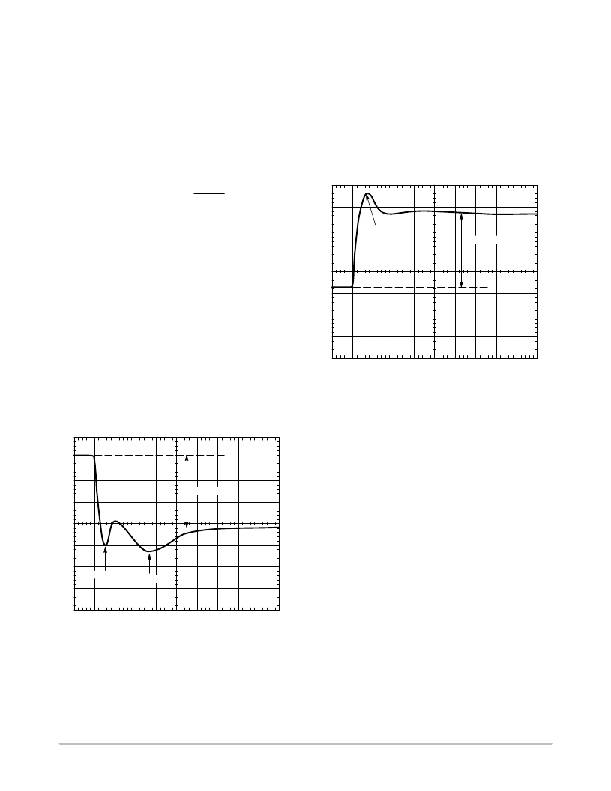
�15.� Users� should� see� a� waveform� that� is� similar� to� the�
�one� in� Figure� 33.� Use� the� horizontal� cursors� to�
�measure� V� ACDRP� and� V� DCDRP� as� shown.� Do� not�
�measure� the� undershoot� or� overshoot� that� occurs�
�immediately� after� the� step.�
�16.� If� the� V� ACDRP� and� V� DCDRP� are� different� by� more�
�than� a� couple� of� mV,� use� the� following� to� adjust� C� CS� .�
�(Note� that� users� may� need� to� parallel� different� values�
�to� get� the� right� one� due� to� the� limited� standard�
�capacitor� values� available.� It� is� also� wise� to� have�
�locations� for� two� capacitors� in� the� layout� for� this.)�
�V� ACDRP�
�(eq.� 44)�
�b.� For� V� TRAN1� ,� increase� C� B� or� increase� switching�
�frequency.�
�c.� For� V� TRAN2� ,� increase� R� A� and� decrease� C� A� ,�
�both� by� 25%.�
�21.� For� load� release� (see� Figure� 34),� if� V� TRANREL� is�
�larger� than� the� IMVP� ?� 6� specification,� there� is� not�
�enough� output� capacitance.� Either� more�
�capacitance� is� needed� or� the� inductor� values� need�
�to� be� smaller.� If� the� inductors� are� changed,� then�
�start� the� design� over� using� Equations� 1� to� 38� and�
�this� tuning� guide.�
�17.� Repeat� Step� 15� and� Step� 16.� Repeat� adjustments� if�
�necessary.� Once� completed,� do� not� change� C� CS� for�
�the� rest� of� the� procedure.�
�18.� Set� dynamic� load� step� to� maximum� step� size.� Do� not�
�use� a� step� size� larger� than� needed.� Verify� that� the�
�output� waveform� is� square,� which� means� V� ACDRP�
�and� V� DCDRP� are� equal.� Note:� Make� sure� that� the�
�load� step� slew� rate� and� turn� ?� on� are� set� for� a� slew�
�rate� of� ~150� A/� m� s� to� 250� A/� m� s� (for� example,� a� load�
�step� of� 50� A� should� take� 200� ns� to� 300� ns)� with� no�
�overshoot.� Some� dynamic� loads� have� an� excessive�
�turn� ?� on� overshoot� if� a� minimum� current� is� not� set�
�properly� (this� is� an� issue� if� using� a� V� TT� tool).�
�V� TRANREL�
�V� DROOP�
�Initial� Transient� Setting�
�19.� With� dynamic� load� still� set� at� the� maximum� step�
�size,� expand� the� scope� time� scale� to� see� 2� m� s/div� to�
�5� m� s/div.� A� waveform� that� has� two� overshoots� and�
�one� minor� undershoot� can� result� (see� Figure� 33).�
�Here,� V� DROOP� is� the� final� desired� value.�
�V� DROOP�
�Figure� 34.� Transient� Setting� Waveform,� Load� Release�
�Layout� and� Component� Placement�
�The� following� guidelines� are� recommended� for� optimal�
�performance� of� a� switching� regulator� in� a� PC� system.�
�General� Recommendations�
�For� effective� results,� at� least� a� 4� ?� layer� PCB� is�
�recommended.� This� allows� the� needed� versatility� for� control�
�circuitry� interconnections� with� optimal� placement,� power�
�planes� for� ground,� input� and� output� power,� and� wide�
�interconnection� traces� in� the� rest� of� the� power� delivery� current�
�paths.� Note� that� each� square� unit� of� 1� ounce� copper� trace� has�
�a� resistance� of� ~0.53� m� W� at� room� temperature.�
�When� high� currents� need� to� be� routed� between� PCB� layers,�
�vias� should� be� used� liberally� to� create� several� parallel� current�
�paths� so� that� the� resistance� and� inductance� introduced� by�
�V� TRAN1�
�V� TRAN2�
�these� current� paths� are� minimized,� and� the� via� current� rating�
�is� not� exceeded.�
�If� critical� signal� lines� (including� the� output� voltage� sense�
�lines� of� the� ADP3207C)� must� cross� through� power� circuitry,�
�Figure� 33.� Transient� Setting� Waveform,� Load� Step�
�20.� If� both� overshoots� are� larger� than� desired,� make�
�the� following� adjustments� in� the� order� they� appear.�
�Note� that� if� these� adjustments� do� not� change� the�
�response,� users� are� limited� by� the� output�
�decoupling.� In� addition,� check� the� output� response�
�each� time� a� change� is� made,� as� well� as� the�
�switching� nodes� to� make� sure� they� are� still� stable.�
�a.� Make� ramp� resistor� larger� by� 25%� (R� RAMP� ).�
�a� signal� ground� plane� should� be� interposed� between� those�
�signal� lines� and� the� traces� of� the� power� circuitry.� This� serves�
�as� a� shield� to� minimize� noise� injection� into� the� signals� at� the�
�expense� of� making� signal� ground� a� bit� noisier.�
�An� analog� ground� plane� should� be� used� around� and� under�
�the� ADP3207C� for� referencing� the� components� associated�
�with� the� controller.� Tie� this� plane� to� the� nearest� output�
�decoupling� capacitor� ground.� It� should� not� be� tied� to� any� other�
�power� circuitry� to� prevent� power� currents� from� flowing� in� it.�
�http://onsemi.com�
�30�
�相关PDF资料 |
PDF描述 |
|---|---|
| ADP3207DJCPZ-RL | IC CTLR BUCK 7BIT MULTI 40LFCSP |
| ADP3208CJCPZ-RL | IC CTLR BUCK 7BIT IMVP6 48LFCSP |
| ADP3208DJCPZ-RL | IC CTLR BUCK 7BIT 2PHASE 48LFCSP |
| ADP320ACPZ-110-R7 | IC REG LDO 3.3/3.3/1.5V 16LFCSP |
| ADP3210MNR2G | IC CTLR BUCK 7BIT MULTIPH 40QFN |
相关代理商/技术参数 |
参数描述 |
|---|---|
| ADP3207D | 制造商:ONSEMI 制造商全称:ON Semiconductor 功能描述:7-Bit Programmable, Multi-Phase Mobile, CPU Synchronous Buck |
| ADP3207DJCPZ-RL | 功能描述:DC/DC 开关控制器 IMVP6 BUCK CONTROLLER RoHS:否 制造商:Texas Instruments 输入电压:6 V to 100 V 开关频率: 输出电压:1.215 V to 80 V 输出电流:3.5 A 输出端数量:1 最大工作温度:+ 125 C 安装风格: 封装 / 箱体:CPAK |
| ADP3207JCPZ-RL | 功能描述:DC/DC 开关控制器 IMVP6 MLTI/PHSE CNTR RoHS:否 制造商:Texas Instruments 输入电压:6 V to 100 V 开关频率: 输出电压:1.215 V to 80 V 输出电流:3.5 A 输出端数量:1 最大工作温度:+ 125 C 安装风格: 封装 / 箱体:CPAK |
| ADP3208AJCPZ-RL | 功能描述:肖特基二极管与整流器 IMVP6 MLT-PH CTRL W/DRVR RoHS:否 制造商:Skyworks Solutions, Inc. 产品:Schottky Diodes 峰值反向电压:2 V 正向连续电流:50 mA 最大浪涌电流: 配置:Crossover Quad 恢复时间: 正向电压下降:370 mV 最大反向漏泄电流: 最大功率耗散:75 mW 工作温度范围:- 65 C to + 150 C 安装风格:SMD/SMT 封装 / 箱体:SOT-143 封装:Reel |
| ADP3208C | 制造商:ONSEMI 制造商全称:ON Semiconductor 功能描述:7-Bit,Programmable,Dual- Phase,Mobile,CPU,Synchronous Buck Controller |
发布紧急采购,3分钟左右您将得到回复。