- 您现在的位置:买卖IC网 > PDF目录11806 > ADP5585ACBZ-00-R7 (Analog Devices Inc)IC PORT EXPANDER 10I/O 16WLSCP PDF资料下载
参数资料
| 型号: | ADP5585ACBZ-00-R7 |
| 厂商: | Analog Devices Inc |
| 文件页数: | 40/40页 |
| 文件大小: | 0K |
| 描述: | IC PORT EXPANDER 10I/O 16WLSCP |
| 标准包装: | 1 |
| 应用: | 小键盘输入,输入/输出扩展 |
| 接口: | I²C |
| 封装/外壳: | 16-UFBGA,WLCSP |
| 供应商设备封装: | 16-WLCSP(1.59x1.59) |
| 包装: | 标准包装 |
| 安装类型: | 表面贴装 |
| 其它名称: | ADP5585ACBZ-00-R7DKR |
第1页第2页第3页第4页第5页第6页第7页第8页第9页第10页第11页第12页第13页第14页第15页第16页第17页第18页第19页第20页第21页第22页第23页第24页第25页第26页第27页第28页第29页第30页第31页第32页第33页第34页第35页第36页第37页第38页第39页当前第40页
Data Sheet
ADP5585
Rev. C | Page 9 of 40
FUNCTIONAL DESCRIPTION
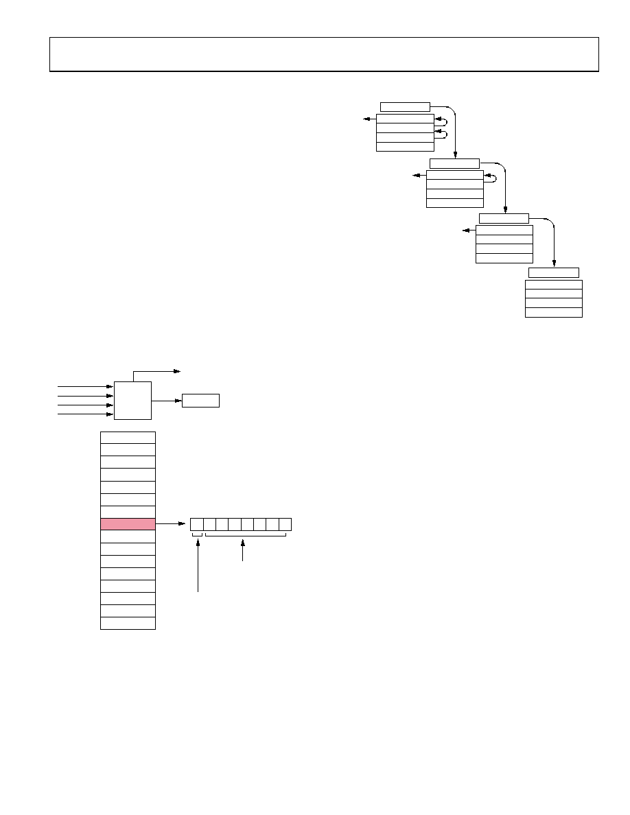
EVENT FIFO
Before going into detail on the various ADP5585 blocks, it is
important to understand the function of the event FIFO. The
ADP5585 features an event FIFO that can record as many as 16
events. By default, the FIFO primarily records key events, such as
key press and key release. However, it is possible to configure
the general-purpose input (GPI) and logic activity to generate
event information on the FIFO as well. An event count, EC[4:0],
is composed of five bits and works in tandem with the FIFO so
that the user knows how much of the FIFO must be read back at
any given time.
The FIFO is composed of 16 eight-bit sections that the user
accesses by reading the FIFO_x registers. The actual FIFO is
not in user accessible registers until a read occurs. The FIFO
can be thought of as a “first in first out” buffer that is used to
fill Register 0x03 to Register 0x12.
The event FIFO is made up of 16 eight-bit registers. In each
register, Bits[6:0] hold the event identifier, and Bit 7 holds the
event state. With seven bits, 127 different events can be identified.
See Table 11 for event decoding.
EVENT1[7:0]
EVENT8_IDENTIFIER[6:0]
EVENT2[7:0]
EVENT3[7:0]
EVENT4[7:0]
EVENT13[7:0]
EVENT14[7:0]
EVENT15[7:0]
EVENT16[7:0]
EVENT5[7:0]
EVENT6[7:0]
EVENT7[7:0]
EVENT8[7:0]
EVENT9[7:0]
EVENT10[7:0]
EVENT11[7:0]
EVENT12[7:0]
7
EVENT8_STATE
GPI EVENTS
EC[4:0]
OVRFLOW_INT
KEY EVENTS
LOGIC EVENTS
6
5
4
3
2
1
0
09841-
006
FIFO
UPDATE
Figure 7. Breakdown of Eventx[7:0] Bits
When events are available on the FIFO, the user should first
read back the event count, EC[4:0], to determine how many
events must be read back. Events can be read from the top of
the FIFO only. When an event is read back, all remaining events
in the FIFO are shifted up one location, and the EC[4:0] count
is decremented.
KEY 3 PRESSED
KEY 3 RELEASED
GPI 7 ACTIVE
EC = 3
KEY 3 RELEASED
GPI 7 ACTIVE
EC = 2
GPI 7 ACTIVE
EC = 1
EC = 0
09841-
007
THIRD
READ
SECOND
READ
FIRST
READ
Figure 8. FIFO Operation
The FIFO registers (0x03 to 0x12) always point to the top of the
FIFO (that is, the location of EVENT1[7:0]). If the user tries to
read back from any location in a FIFO, data is always obtained
from the top of that FIFO. This ensures that events can only be
read back in the order in which they occurred, thus ensuring
the integrity of the FIFO system.
As stated above, some of the onboard functions of ADP5585
can be programmed to generate events on the FIFO. A FIFO
update control block manages updates to the FIFO. If an I2C
transaction is accessing any of the FIFO address locations,
updates are paused until the I2C transaction has completed.
A FIFO overflow event occurs when more than 16 events are
generated prior to an external processor reading a FIFO and
clearing it.
If an overflow condition occurs, the overflow status bit is set.
An interrupt is generated if overflow interrupt is enabled,
signaling to the processor that more than 16 events have
occurred.
KEY SCAN CONTROL
General
The 10 input/output pins can be configured to decode a keypad
matrix up to a maximum size of 25 switches (5 × 5 matrix). Smaller
matrices can also be configured, freeing up the unused row and
column pins for other I/O functions.
The R0 through R4 I/O pins comprise the rows of the keypad
matrix. The C0 through C4 I/O pins comprise the columns of
the keypad matrix. Pins used as rows are pulled up via the internal
300 kΩ (or 100 kΩ) resistors. Pins used as columns are driven
low via the internal NMOS current sink.
相关PDF资料 |
PDF描述 |
|---|---|
| 0533980471 | CONN HEADER 4POS 1.25MM VERT SMD |
| 1604398-2 | CONN 1-POLE MODULAR 1/0 AWG BLCK |
| 1604398-4 | CONN 1-POLE MODULAR 1/0 AWG RED |
| TXS02326RGER | IC SIM CARD MUX 2:1 24VQFN |
| MS3114E12-8PW | CONN RCPT 8POS JAM NUT W/PINS |
相关代理商/技术参数 |
参数描述 |
|---|---|
| ADP5585ACBZ-01-R7 | 功能描述:IC PORT EXPANDER 10I/O 16WLSCP RoHS:是 类别:集成电路 (IC) >> 接口 - 专用 系列:- 特色产品:NXP - I2C Interface 标准包装:1 系列:- 应用:2 通道 I²C 多路复用器 接口:I²C,SM 总线 电源电压:2.3 V ~ 5.5 V 封装/外壳:16-TSSOP(0.173",4.40mm 宽) 供应商设备封装:16-TSSOP 包装:剪切带 (CT) 安装类型:表面贴装 产品目录页面:825 (CN2011-ZH PDF) 其它名称:568-1854-1 |
| ADP5585ACBZ-02-R7 | 功能描述:IC PORT EXPANDER 10I/O 16WLSCP RoHS:是 类别:集成电路 (IC) >> 接口 - 专用 系列:- 特色产品:NXP - I2C Interface 标准包装:1 系列:- 应用:2 通道 I²C 多路复用器 接口:I²C,SM 总线 电源电压:2.3 V ~ 5.5 V 封装/外壳:16-TSSOP(0.173",4.40mm 宽) 供应商设备封装:16-TSSOP 包装:剪切带 (CT) 安装类型:表面贴装 产品目录页面:825 (CN2011-ZH PDF) 其它名称:568-1854-1 |
| ADP5585ACBZ-04-R7 | 制造商:AD 制造商全称:Analog Devices 功能描述:Keypad Decoder and I/O Expansion |
| ADP5585ACPZ-00-R7 | 功能描述:IC PORT EXPANDER 10I/O 16LFCSP RoHS:是 类别:集成电路 (IC) >> 接口 - 专用 系列:* 特色产品:NXP - I2C Interface 标准包装:1 系列:- 应用:2 通道 I²C 多路复用器 接口:I²C,SM 总线 电源电压:2.3 V ~ 5.5 V 封装/外壳:16-TSSOP(0.173",4.40mm 宽) 供应商设备封装:16-TSSOP 包装:剪切带 (CT) 安装类型:表面贴装 产品目录页面:825 (CN2011-ZH PDF) 其它名称:568-1854-1 |
| ADP5585ACPZ-01-R7 | 功能描述:IC PORT EXPANDER 10I/O 16LFCSP RoHS:是 类别:集成电路 (IC) >> 接口 - 专用 系列:* 特色产品:NXP - I2C Interface 标准包装:1 系列:- 应用:2 通道 I²C 多路复用器 接口:I²C,SM 总线 电源电压:2.3 V ~ 5.5 V 封装/外壳:16-TSSOP(0.173",4.40mm 宽) 供应商设备封装:16-TSSOP 包装:剪切带 (CT) 安装类型:表面贴装 产品目录页面:825 (CN2011-ZH PDF) 其它名称:568-1854-1 |
发布紧急采购,3分钟左右您将得到回复。