- 您现在的位置:买卖IC网 > PDF目录17040 > ADS1259EVM (Texas Instruments)EVAL MODULE FOR ADS1259 PDF资料下载
参数资料
| 型号: | ADS1259EVM |
| 厂商: | Texas Instruments |
| 文件页数: | 19/48页 |
| 文件大小: | 0K |
| 描述: | EVAL MODULE FOR ADS1259 |
| 标准包装: | 1 |
| ADC 的数量: | 1 |
| 位数: | 24 |
| 采样率(每秒): | 14k |
| 数据接口: | 串行,SPI? |
| 工作温度: | -40°C ~ 125°C |
| 已用 IC / 零件: | ADS1259 |
| 已供物品: | 板 |
| 其它名称: | 296-29312 ADS1259EVM-ND |
第1页第2页第3页第4页第5页第6页第7页第8页第9页第10页第11页第12页第13页第14页第15页第16页第17页第18页当前第19页第20页第21页第22页第23页第24页第25页第26页第27页第28页第29页第30页第31页第32页第33页第34页第35页第36页第37页第38页第39页第40页第41页第42页第43页第44页第45页第46页第47页第48页
FinalOutputData=(Input
OFC[2:0])
-
FSC[2:0]
400000h
Modulator
AINP
AINN
Digital
Filter
S
OFC
Register
FinalOutput
OutputData
Clippedto24Bits
+
-
FSCRegister
400000h
SBAS424D
– JUNE 2009 – REVISED AUGUST 2011
Table 11. Offset Calibration Values
OFFSET AND FULL-SCALE CALIBRATION
REGISTERS
OFC REGISTER
FINAL OUTPUT CODE(1)
7FFFFFh
800001h
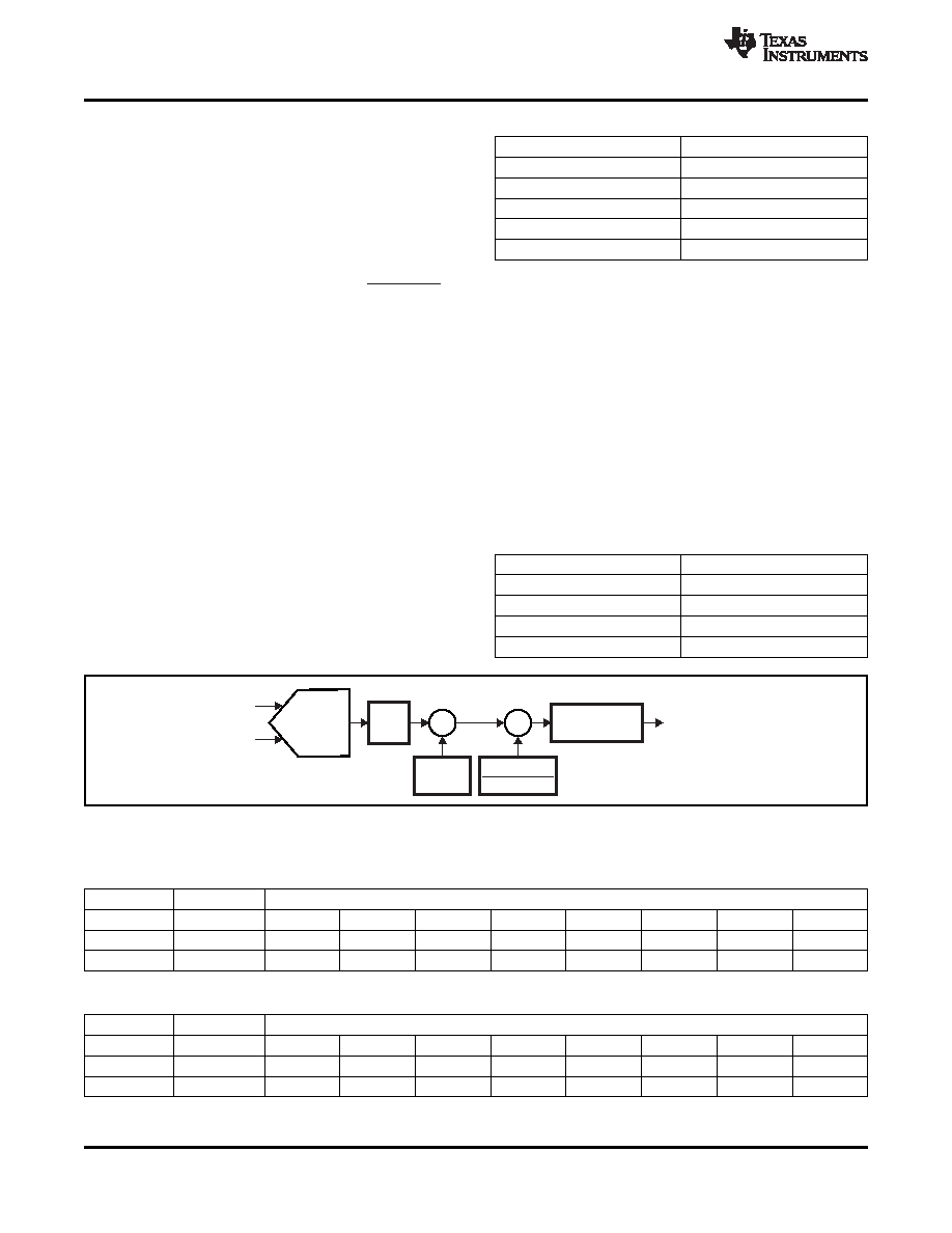
The conversion data are scaled by offset and gain
registers before yielding the final output code. As
000001h
FFFFFFh
shown in Figure 55, the output of the digital filter is
000000h
first subtracted by the offset register (OFC) and then
FFFFFFh
000001h
multiplied by the full-scale register (FSC). Equation 8
800001h
7FFFFFh
shows the scaling:
(1) Ideal output code excluding noise and inherent offset error.
FSC[2:0] Registers
(8)
The full-scale calibration is a 24-bit word, composed
The values of the offset and full-scale registers are
of three 8-bit registers, as shown in Table 14. The
set by writing to them directly, or they are set by
full-scale calibration value is 24-bit, straight binary,
calibration commands.
normalized to 1.0 at code 400000h. Table 12
summarizes the scaling of the full-scale register. A
OFC[2:0] Registers
register value of 400000h (default value) has no gain
The offset calibration is a 24-bit word, composed of
correction (gain = 1). Note that while the gain
three 8-bit registers, as shown in Table 13. The offset
calibration register value corrects gain errors above 1
is in twos complement format with a maximum
(gain correction
< 1), the full-scale range of the
positive value of 7FFFFFh and a maximum negative
analog inputs cannot exceed 105% full-scale to avoid
value of 800000h. This value is subtracted from the
input overload.
conversion data. A register value of 00000h has no
offset correction (default value). Note that while the
Table 12. Full-Scale Calibration Register Values
offset calibration register value can correct offsets
FSC REGISTER
GAIN FACTOR
ranging from
–FS to +FS (as Table 11 shows), to
800000h
2.0
avoid input overload, the analog inputs cannot
exceed 105% full-scale.
400000h
1.0
200000h
0.5
000000h
0
Figure 55. Calibration Block Diagram
Table 13. Offset Calibration Word
REGISTER
BYTE
BIT ORDER
OFC0
LSB
B7
B6
B5
B4
B3
B2
B1
B0 (LSB)
OFC1
MID
B15
B14
B13
B12
B11
B10
B9
B8
OFC2
MSB
B23 (MSB)
B22
B21
B20
B19
B18
B17
B16
Table 14. Full-Scale Calibration Word
REGISTER
BYTE
BIT ORDER
FSC0
LSB
B7
B6
B5
B4
B3
B2
B1
B0 (LSB)
FSC1
MID
B15
B14
B13
B12
B11
B10
B9
B8
FSC2
MSB
B23 (MSB)
B22
B21
B20
B19
B18
B17
B16
26
Copyright
2009–2011, Texas Instruments Incorporated
相关PDF资料 |
PDF描述 |
|---|---|
| 0210490281 | CABLE JUMPER 1.25MM .076M 22POS |
| EBC19DREN-S93 | CONN EDGECARD 38POS .100 EYELET |
| EEC19DRYN-S93 | CONN EDGECARD 38POS DIP .100 SLD |
| EBC19DREH-S93 | CONN EDGECARD 38POS .100 EYELET |
| MLK1005S2N4S | INDUCTOR MULTILAYER 2.4NH 0402 |
相关代理商/技术参数 |
参数描述 |
|---|---|
| ADS1259EVM | 制造商:Texas Instruments 功能描述:DEVELOPMENT TOOL |
| ADS1259EVM-PDK | 功能描述:数据转换 IC 开发工具 ADS1259 Perf Demo Kit RoHS:否 制造商:Texas Instruments 产品:Demonstration Kits 类型:ADC 工具用于评估:ADS130E08 接口类型:SPI 工作电源电压:- 6 V to + 6 V |
| ADS1259EVM-PDK | 制造商:Texas Instruments 功能描述:DEVELOPMENT TOOL |
| ADS1259IPW | 功能描述:模数转换器 - ADC Low-Noise 14kSPS 24B ADC RoHS:否 制造商:Texas Instruments 通道数量:2 结构:Sigma-Delta 转换速率:125 SPs to 8 KSPs 分辨率:24 bit 输入类型:Differential 信噪比:107 dB 接口类型:SPI 工作电源电压:1.7 V to 3.6 V, 2.7 V to 5.25 V 最大工作温度:+ 85 C 安装风格:SMD/SMT 封装 / 箱体:VQFN-32 |
| ADS1259IPW | 制造商:Texas Instruments 功能描述:A/D CONVERTER (A-D) IC |
发布紧急采购,3分钟左右您将得到回复。