- 您现在的位置:买卖IC网 > PDF目录17040 > ADS1259EVM (Texas Instruments)EVAL MODULE FOR ADS1259 PDF资料下载
参数资料
| 型号: | ADS1259EVM |
| 厂商: | Texas Instruments |
| 文件页数: | 22/48页 |
| 文件大小: | 0K |
| 描述: | EVAL MODULE FOR ADS1259 |
| 标准包装: | 1 |
| ADC 的数量: | 1 |
| 位数: | 24 |
| 采样率(每秒): | 14k |
| 数据接口: | 串行,SPI? |
| 工作温度: | -40°C ~ 125°C |
| 已用 IC / 零件: | ADS1259 |
| 已供物品: | 板 |
| 其它名称: | 296-29312 ADS1259EVM-ND |
第1页第2页第3页第4页第5页第6页第7页第8页第9页第10页第11页第12页第13页第14页第15页第16页第17页第18页第19页第20页第21页当前第22页第23页第24页第25页第26页第27页第28页第29页第30页第31页第32页第33页第34页第35页第36页第37页第38页第39页第40页第41页第42页第43页第44页第45页第46页第47页第48页
+V
REF
(2
1)
-
23
-VREF
(2
1)
-
23
MSB
MID
LSB
CHECKSUM
Bit7ofChecksum
or
Flag=1;Bit0ofLSBConversionData
24-BitConversionData(CHKSUM=0)
32-BitConversionData (CHKSUM=1)
-VREF
2
23
2
1
-
23
SBAS424D
– JUNE 2009 – REVISED AUGUST 2011
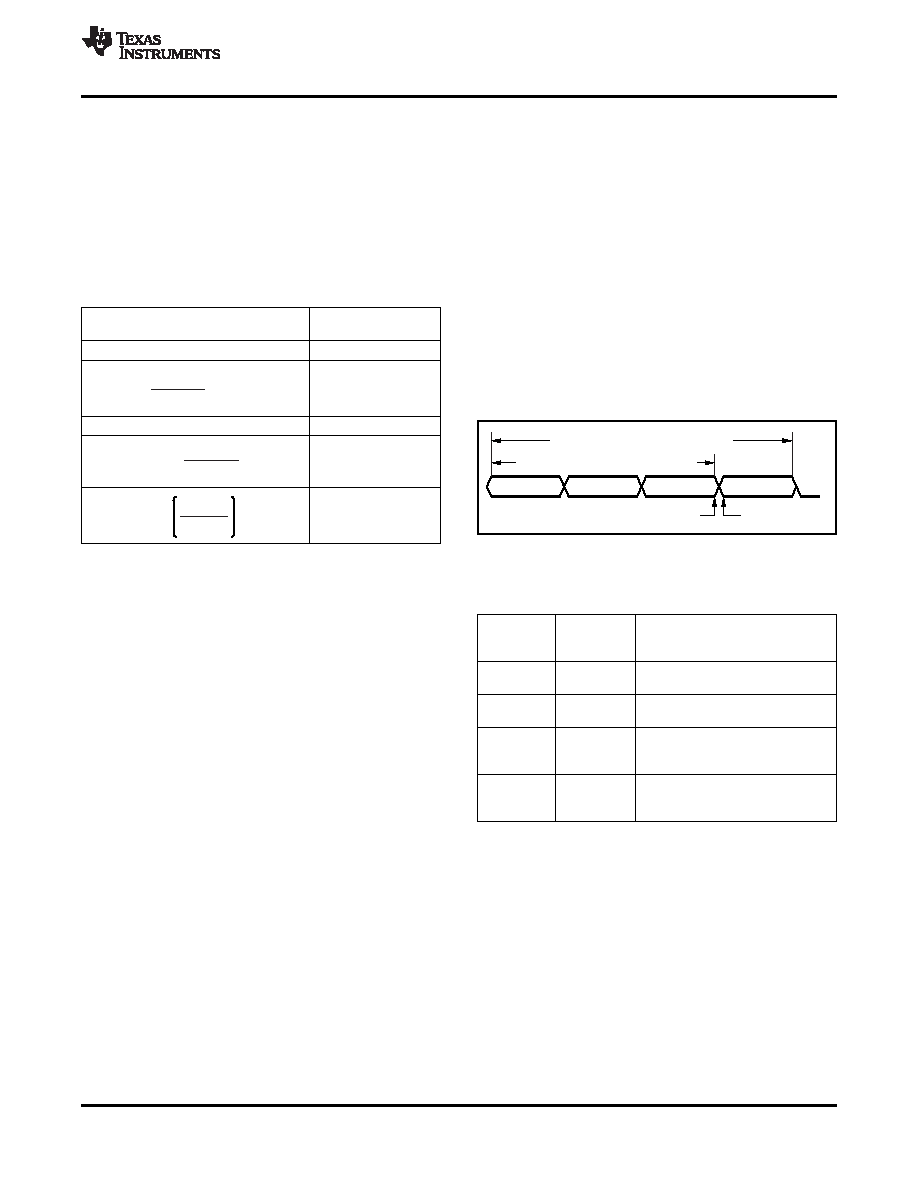
DATA FORMAT
DATA CHECKSUM BYTE AND FLAG BIT
The ADS1259 outputs 24 bits of conversion data in
An optional checksum byte can be appended to the
binary twos complement format, MSB first. The data
conversion data bytes. The checksum makes the
LSB has a weight of VREF/(2
23
– 1). A positive
data word length four bytes in length instead of three.
full-scale input produces an output code of 7FFFFFh
The checksum byte is enabled by the register bit
and the negative full-scale input produces an output
CHKSUM. The checksum itself is the least significant
code of 800000h. The output clips at these codes for
byte sum of the three conversion data bytes, offset by
signals that exceed full-scale. Table 16 summarizes the
9Bh. Note that the checksum byte option only applies
ideal output codes for different input signals.
to the readback conversion data, not to register data.
The checksum is either seven bits or eight bits,
Table 16. Ideal Output Code versus Input Signal
depending if the FLAG register bit is enabled. If the
FLAG bit is enabled the checksum is seven bits, with
DIFFERENTIAL INPUT SIGNAL VIN
IDEAL OUTPUT
bit 7 replaced by the out-of-range flag. Figure 58 and
(AINP
– AINN)
Table 17 describe the combinations of the FLAG and
≥ VREF
7FFFFFh
CHKSUM register bits.
Checksum = MSB data byte + Mid data byte + LSB
000001h
data byte + 9Bh.
0
000000h
FFFFFFh
800000h
Figure 58. Checksum Byte and Out-of-Range Flag
(1) Excludes effects of noise, linearity, offset, and gain errors.
DATA INTEGRITY
Table 17. Checksum Byte and Over-Range Flag
Data readback integrity is augmented by a checksum
FLAG
CHKSUM
byte
and
redundant
data
read
capability.
The
REGISTER
checksum byte is the sum of three data conversion
BIT
DESCRIPTION
bytes, offset by 9Bh. Additionally, the data conversion
No checksum byte, no out-of-range
0
bytes may be read multiple times by continuing to
flag
shift data past the initial read of 24 bits (32 bits if
8-bit checksum byte, no
0
1
checksum is enabled).
out-of-range flag
No checksum byte, out-of-range
1
0
flag replaces LSB (bit 0) of
conversion data
7-bit checksum byte, out-of-range
1
replaces MSB (bit 7) of checksum
byte.
Copyright
2009–2011, Texas Instruments Incorporated
29
相关PDF资料 |
PDF描述 |
|---|---|
| 0210490281 | CABLE JUMPER 1.25MM .076M 22POS |
| EBC19DREN-S93 | CONN EDGECARD 38POS .100 EYELET |
| EEC19DRYN-S93 | CONN EDGECARD 38POS DIP .100 SLD |
| EBC19DREH-S93 | CONN EDGECARD 38POS .100 EYELET |
| MLK1005S2N4S | INDUCTOR MULTILAYER 2.4NH 0402 |
相关代理商/技术参数 |
参数描述 |
|---|---|
| ADS1259EVM | 制造商:Texas Instruments 功能描述:DEVELOPMENT TOOL |
| ADS1259EVM-PDK | 功能描述:数据转换 IC 开发工具 ADS1259 Perf Demo Kit RoHS:否 制造商:Texas Instruments 产品:Demonstration Kits 类型:ADC 工具用于评估:ADS130E08 接口类型:SPI 工作电源电压:- 6 V to + 6 V |
| ADS1259EVM-PDK | 制造商:Texas Instruments 功能描述:DEVELOPMENT TOOL |
| ADS1259IPW | 功能描述:模数转换器 - ADC Low-Noise 14kSPS 24B ADC RoHS:否 制造商:Texas Instruments 通道数量:2 结构:Sigma-Delta 转换速率:125 SPs to 8 KSPs 分辨率:24 bit 输入类型:Differential 信噪比:107 dB 接口类型:SPI 工作电源电压:1.7 V to 3.6 V, 2.7 V to 5.25 V 最大工作温度:+ 85 C 安装风格:SMD/SMT 封装 / 箱体:VQFN-32 |
| ADS1259IPW | 制造商:Texas Instruments 功能描述:A/D CONVERTER (A-D) IC |
发布紧急采购,3分钟左右您将得到回复。