- 您现在的位置:买卖IC网 > PDF目录10606 > ADS62P44IRGCT (Texas Instruments)IC ADC 14BIT DUAL 105MSPS 64VQFN PDF资料下载
参数资料
| 型号: | ADS62P44IRGCT |
| 厂商: | Texas Instruments |
| 文件页数: | 78/78页 |
| 文件大小: | 0K |
| 描述: | IC ADC 14BIT DUAL 105MSPS 64VQFN |
| 产品培训模块: | Data Converter Basics |
| 标准包装: | 1 |
| 位数: | 14 |
| 采样率(每秒): | 105M |
| 数据接口: | 串行,并联 |
| 转换器数目: | 2 |
| 电压电源: | 模拟和数字 |
| 工作温度: | -40°C ~ 85°C |
| 安装类型: | 表面贴装 |
| 封装/外壳: | 64-VFQFN 裸露焊盘 |
| 供应商设备封装: | 64-VQFN 裸露焊盘(9x9) |
| 包装: | 标准包装 |
| 输入数目和类型: | 2 个差分,单极 |
| 其它名称: | 296-23137-6 |
第1页第2页第3页第4页第5页第6页第7页第8页第9页第10页第11页第12页第13页第14页第15页第16页第17页第18页第19页第20页第21页第22页第23页第24页第25页第26页第27页第28页第29页第30页第31页第32页第33页第34页第35页第36页第37页第38页第39页第40页第41页第42页第43页第44页第45页第46页第47页第48页第49页第50页第51页第52页第53页第54页第55页第56页第57页第58页第59页第60页第61页第62页第63页第64页第65页第66页第67页第68页第69页第70页第71页第72页第73页第74页第75页第76页第77页当前第78页
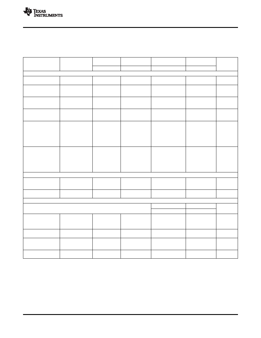
SLAS561C
– JULY 2007 – REVISED FEBRUARY 2012
TIMING CHARACTERISTICS
– LVDS AND CMOS MODES
(continued)
Typical values are specified at 25
°C, AVDD = DRVDD = 3.3 V, maximum rated sampling frequency, sine wave input clock,
1.5 VPP clock amplitude, CL = 5 pF
(2), I
O = 3.5 mA, RL = 100
(3), no internal termination, unless otherwise noted.
Min and max values are specified across the full temperature range TMIN = –40°C to TMAX = 85°C, AVDD = 3.0 V to 3.6 V,
unless otherwise specified.
ADS62P45
ADS62P44
ADS62P43
ADS62P42
FS = 125 MSPS
FS = 105 MSPS
FS = 80 MSPS
FS = 65 MSPS
PARAMETER
TEST CONDITIONS
UNIT
MIN
TYP
MAX
MIN
TYP
MAX
MIN
TYP
MAX
MIN
TYP
MAX
PARALLEL CMOS MODE, DRVDD = 2.5 V to 3.6 V, default output buffer drive strength (7)
Data setup
Data valid(8) to 50% of
tsu
2.0
3.5
2.8
4.3
5.8
5.7
7.2
ns
time(5)
CLKOUT rising edge
50% of CLKOUT
Data hold
th
rising edge to data
2.0
3.5
2.7
4.2
5.7
5.6
7.1
ns
time(5)
becoming invalid(8)
Clock
Input clock rising edge
tPDI
propagation
zero-cross to 50% of
5.8
7.3
8.8
5.8
7.3
8.8
5.8
7.3
8.8
5.8
7.3
8.8
ns
delay
CLKOUT rising edge
Duty cycle of output
Output clock
clock (CLKOUT)
45% 53%
60%
45% 53%
60%
45%
53%
60% 45%
53%
60%
duty cycle
10
≤ Fs ≤ 125 MSPS
Rise time measured
from 20% to 80% of
Data rise
DRVDD
tr
time
Fall time measured
1.0
1.8
2.5
1.0
1.8
2.5
1.0
1.8
2.5
1.0
1.8
2.5
ns
tf
Data fall
from 80% to 20% of
time
DRVDD
1
≤ Fs ≤ 125 MSPS
Rise time measured
from 20% to 80% of
Output clock
DRVDD
tCLKRISE
rise time
Fall time measured
1.0
1.8
2.5
1.0
1.8
2.5
1.0
1.8
2.5
1.0
1.8
2.5
ns
tCLKFALL
Output clock
from 80% to 20% of
fall time
DRVDD
1
≤ Fs ≤ 125 MSPS
PARALLEL CMOS INTERFACE, DRVDD = 1.8V, maximum buffer drive strength(9)
Input clock rising edge
tSTART
Start time
to data getting valid
8.5
7.5
5.5
3.6
ns
(10) (11)
Width of valid data
tDV
3.3
6.0
5.0
7.5
8.0
10.5
13.5
ns
window
PARALLEL CMOS INTERFACE, DRVDD = 1.8V, MULTIPLEXED MODE, maximum buffer drive strength
FS = 65 MSPS
FS = 40 MSPS
UNIT
MIN
TYP
MAX
MIN
TYP
MAX
Input clock falling
Start time,
edge to channel A
tSTART_CHA
0.8
2.3
–4.5
–3
ns
channel A
data getting valid(10)
(11)
Data valid,
Width of valid data
tDV_CHA
5.4
6.4
10.3
11.3
ns
channel A
window
Input clock rising edge
Start time,
tSTART_CHB
to channel B data
1.1
2.4
–4.1
–2.5
ns
channel B
getting valid (10) (11)
Data valid,
Width of valid data
tDV_CHB
5
6
9.7
10.7
ns
channel B
window
(7)
For DRVDD
< 2.2 V, it is recommended to use external clock for data capture and NOT the device output clock signal (CLKOUT). See
Parallel CMOS interface in application section.
(8)
Data valid refers to logic high of 2 V (1.7 V) and logic low of 0.8 V (0.7 V) for DRVDD = 3.3 V (2.5 V).
(9)
For DRVDD
< 2.2 V, output clock cannot be used for data capture. A delayed version of the input clock can be used, that gives the
desired setup
& hold times at the receiving chip
(10) Data valid refers to LOGIC HIGH of 1.26 V and LOGIC LOW of 0.54 V for DRVDD = 1.8 V
(11) Measured from zero-crossing of input clock having 50% duty cycle
Copyright
2007–2012, Texas Instruments Incorporated
9
Product Folder Link(s): ADS62P45, ADS62P44 ADS62P43, ADS62P42
相关PDF资料 |
PDF描述 |
|---|---|
| VE-B5L-MW | CONVERTER MOD DC/DC 28V 100W |
| 16982-5SG-522 | CONN PLUG 5POS CABLE SKT |
| VE-BW4-IV-F1 | CONVERTER MOD DC/DC 48V 150W |
| VE-B5K-MX-F4 | CONVERTER MOD DC/DC 40V 75W |
| PX0735/P | CONN JAM NUT 2POS W/PINS |
相关代理商/技术参数 |
参数描述 |
|---|---|
| ADS62P44IRGCTG4 | 功能描述:模数转换器 - ADC DUAL 14B 105MSPS Para ADC RoHS:否 制造商:Texas Instruments 通道数量:2 结构:Sigma-Delta 转换速率:125 SPs to 8 KSPs 分辨率:24 bit 输入类型:Differential 信噪比:107 dB 接口类型:SPI 工作电源电压:1.7 V to 3.6 V, 2.7 V to 5.25 V 最大工作温度:+ 85 C 安装风格:SMD/SMT 封装 / 箱体:VQFN-32 |
| ADS62P44RGC | 制造商:TI 制造商全称:Texas Instruments 功能描述:Dual Channel 14-Bit, 125/105/80/65 MSPS ADC with Parallel CMOS/DDR LVDS outputs |
| ADS62P45 | 制造商:TI 制造商全称:Texas Instruments 功能描述:Dual Channel 14-Bit, 125/105/80/65 MSPS ADC with Parallel CMOS/DDR LVDS outputs |
| ADS62P45_08 | 制造商:TI 制造商全称:Texas Instruments 功能描述:DUAL CHANNEL, 14-BITS, 125/105/80/65 MSPS ADC WITH DDR LVDS/CMOS OUTPUTS |
| ADS62P45EVM | 功能描述:数据转换 IC 开发工具 ADS62P25 Eval Mod RoHS:否 制造商:Texas Instruments 产品:Demonstration Kits 类型:ADC 工具用于评估:ADS130E08 接口类型:SPI 工作电源电压:- 6 V to + 6 V |
发布紧急采购,3分钟左右您将得到回复。