- 您现在的位置:买卖IC网 > PDF目录19505 > ADSP-21371KSWZ-2B (Analog Devices Inc)IC DSP 32BIT 266MHZ 208-LQFP PDF资料下载
参数资料
| 型号: | ADSP-21371KSWZ-2B |
| 厂商: | Analog Devices Inc |
| 文件页数: | 9/48页 |
| 文件大小: | 0K |
| 描述: | IC DSP 32BIT 266MHZ 208-LQFP |
| 产品培训模块: | SHARC Processor Overview |
| 标准包装: | 1 |
| 系列: | SHARC® |
| 类型: | 浮点 |
| 接口: | DAI,DPI |
| 时钟速率: | 266MHz |
| 非易失内存: | ROM(512 kB) |
| 芯片上RAM: | 128kB |
| 电压 - 输入/输出: | 3.30V |
| 电压 - 核心: | 1.20V |
| 工作温度: | 0°C ~ 70°C |
| 安装类型: | 表面贴装 |
| 封装/外壳: | 208-LQFP 裸露焊盘 |
| 供应商设备封装: | 208-LQFP-EP(28x28) |
| 包装: | 托盘 |
第1页第2页第3页第4页第5页第6页第7页第8页当前第9页第10页第11页第12页第13页第14页第15页第16页第17页第18页第19页第20页第21页第22页第23页第24页第25页第26页第27页第28页第29页第30页第31页第32页第33页第34页第35页第36页第37页第38页第39页第40页第41页第42页第43页第44页第45页第46页第47页第48页
ADSP-21371
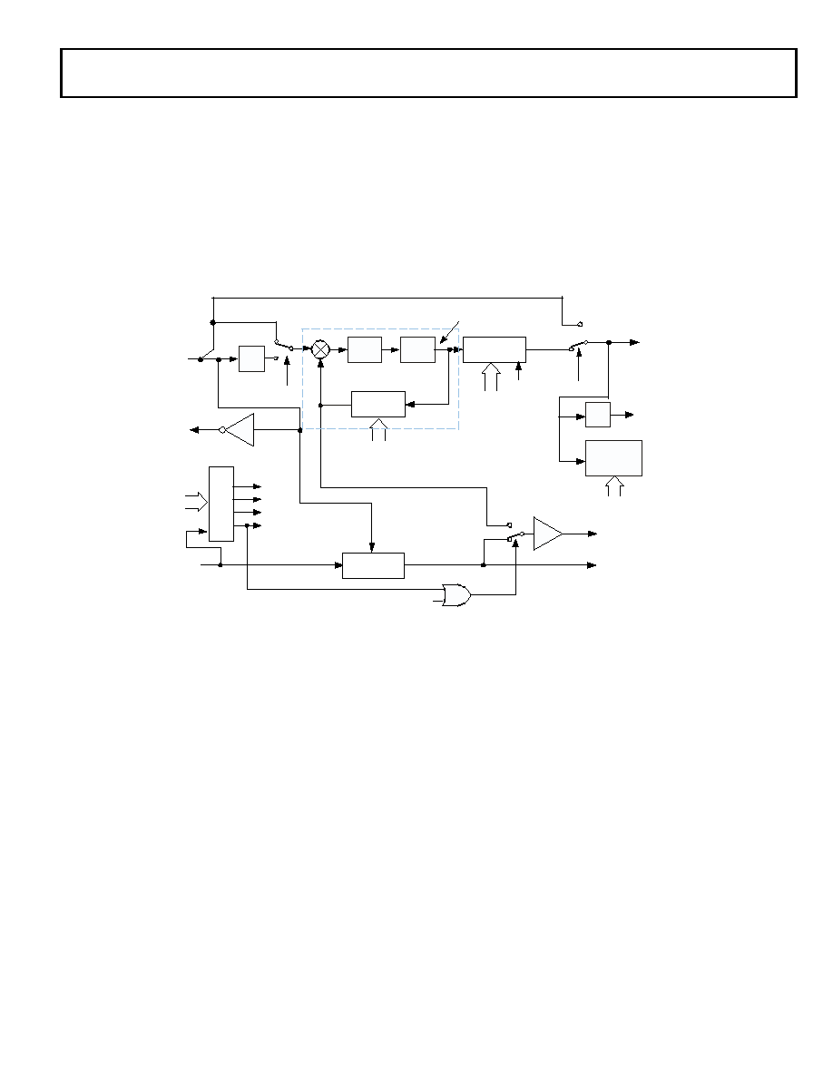
Figure 3 shows core to CLKIN ratios of 6:1, 16:1, and 32:1 with
external oscillator or crystal. Note that more ratios are possible
and can be set through software using the power management
TIMING SPECIFICATIONS
The ADSP-21371’s internal clock (a multiple of CLKIN) pro
vides the clock signal for timing internal memory, processor
core, and serial ports. During reset, program the ratio between
the processor’s internal clock frequency and external (CLKIN)
clock frequency with the CLKCFG1–0 pins (see Table 8 on
Page 14). To determine switching frequencies for the serial
ports, divide down the internal clock, using the programmable
divider control of each port (DIVx for the serial ports).
The ADSP-21371’s internal clock switches at higher frequencies
than the system input clock (CLKIN). To generate the internal
clock, the processor uses an internal phase-locked loop (PLL).
This PLL-based clocking minimizes the skew between the sys
tem clock (CLKIN) signal and the processor’s internal clock.
Core clock frequency can be calculated as:
CCLK = 1
tCCLK = fINPUT
(PLLM/PLLD)
÷2
+
–
0
1
INDIV[8]
LOOP
FILTER
VCO
÷1, 2,4,8
N
PLLD[7..6]
DIVEN[9]
0
1
PLLBP[15]
AMP
÷1-64
M
PLLM[5..0]
C
L
K
_
C
F
G
[1
..
0
]
00 =
6
01 =
32
10 =
16
11 =
6
DELAY
4096
CLKIN
CLKOUTEN[12]
BUFF
÷2
0
1
CCLK
100M Hz
266M Hz
PCLK
(IOP)
CLKOUT
or
CORERST
RSTOUT
CLKIN
3.125M H z
66 .7M H z
RESET
XTAL
@BOOT, CLKCFG[]->PLLM[]
160 M H z < VC O_OU T < 800M H z
÷2, 2.5,
3, 3.5, 4
SDRATIO[20..18]
PLL B YP AS S; R e se r v ed
MULTIPLIER
BLOCK
control register (PMCTL). For more information, see the ADSP
2136x SHARC Processor Programming Reference.
to
SDCLK
Figure 3. Core Clock and System Clock Relationship to CLKIN
Note that in the user application, the PLL multiplier value
should be selected in such a way that the VCO frequency falls in
between 160 MHz and 800 MHz. The VCO frequency is calcu
lated as follows:
where:
fVCO = VCO frequency.
PLLM = multiplier value programmed.
PLLD = divider value programmed.
fINPUT = input frequency to the PLL.
fINPUT = CLKIN when the input divider is disabled.
fINPUT = CLKIN/2 when the input divider is enabled.
C
L
K
F
G
[1
..
0
]
Rev. 0
|
Page 17 of 48
|
June 2007
相关PDF资料 |
PDF描述 |
|---|---|
| RCM10DTKN-S288 | CONN EDGECARD 20POS .156 EXTEND |
| ACM36DSXH | CONN EDGECARD 72POS DIP .156 SLD |
| GA355DR7GB153KY02L | CAP CER 0.015UF 250V 10% 2220 |
| RCM10DTKH-S288 | CONN EDGECARD 20POS .156 EXTEND |
| ADSP-BF536BBCZ-4A | IC DSP CTLR 16BIT 182CSPBGA |
相关代理商/技术参数 |
参数描述 |
|---|---|
| ADSP-21371KSWZ-2B2 | 制造商:AD 制造商全称:Analog Devices 功能描述:SHARC Processor optimized for high performance audio processing |
| ADSP-21371KSWZ-2BX | 制造商:Analog Devices 功能描述:- Trays |
| ADSP-21371KSZ-2A | 制造商:Analog Devices 功能描述:DSP FLOATING PT 32BIT/40-BIT 266MHZ 266MIPS 208MQFP - Trays |
| ADSP-21371KSZ-2B | 制造商:Analog Devices 功能描述:DSP Floating-Point 32-Bit/40-Bit 266MHz 266MIPS 208-Pin MQFP 制造商:Analog Devices 功能描述:DSP FLOATING PT 32BIT/40-BIT 266MHZ 266MIPS 208MQFP - Trays |
| ADSP-21371KSZ-2BX | 制造商:Analog Devices 功能描述:DSP SHARC ADSP-21371 - Trays |
发布紧急采购,3分钟左右您将得到回复。