- 您现在的位置:买卖IC网 > PDF目录19382 > ADSP-2188NKSTZ-320 (Analog Devices Inc)IC DSP CONTROLLER 16BIT 100LQFP PDF资料下载
参数资料
| 型号: | ADSP-2188NKSTZ-320 |
| 厂商: | Analog Devices Inc |
| 文件页数: | 19/48页 |
| 文件大小: | 0K |
| 描述: | IC DSP CONTROLLER 16BIT 100LQFP |
| 标准包装: | 1 |
| 系列: | ADSP-21xx |
| 类型: | 定点 |
| 接口: | 主机接口,串行端口 |
| 时钟速率: | 80MHz |
| 非易失内存: | 外部 |
| 芯片上RAM: | 256kB |
| 电压 - 输入/输出: | 1.8V,2.5V,3.3V |
| 电压 - 核心: | 1.80V |
| 工作温度: | 0°C ~ 70°C |
| 安装类型: | 表面贴装 |
| 封装/外壳: | 100-LQFP |
| 供应商设备封装: | 100-LQFP(14x14) |
| 包装: | 托盘 |
第1页第2页第3页第4页第5页第6页第7页第8页第9页第10页第11页第12页第13页第14页第15页第16页第17页第18页当前第19页第20页第21页第22页第23页第24页第25页第26页第27页第28页第29页第30页第31页第32页第33页第34页第35页第36页第37页第38页第39页第40页第41页第42页第43页第44页第45页第46页第47页第48页
Rev. A
|
Page 26 of 48
|
August 2006
ADSP-218xN
TIMING SPECIFICATIONS
This section contains timing information for the DSP’s
external signals.
General Notes
Use the exact timing information given. Do not attempt to
derive parameters from the addition or subtraction of others.
While addition or subtraction would yield meaningful results
for an individual device, the values given in this data sheet
reflect statistical variations and worst cases. Consequently,
parameters cannot be added up meaningfully to derive
longer times.
Timing Notes
Switching characteristics specify how the processor changes its
signals. Designers have no control over this timing—circuitry
external to the processor must be designed for compatibility
with these signal characteristics. Switching characteristics tell
what the processor will do in a given circumstance. Switching
characteristics can also be used to ensure that any timing
requirement of a device connected to the processor (such as
memory) is satisfied.
Timing requirements apply to signals that are controlled by cir-
cuitry external to the processor, such as the data input for a read
operation. Timing requirements guarantee that the processor
operates correctly with other devices.
Frequency Dependency For Timing Specifications
tCK is defined as 0.5 tCKI. The ADSP-218xN uses an input clock
with a frequency equal to half the instruction rate. For example,
a 40 MHz input clock (which is equivalent to 25 ns) yields a
12.5 ns processor cycle (equivalent to 80 MHz). tCK values
within the range of 0.5 tCKI period should be substituted for all
relevant timing parameters to obtain the specification value.
Example: tCKH = 0.5 tCK – 2 ns = 0.5 (12.5 ns) – 2 ns = 4.25 ns
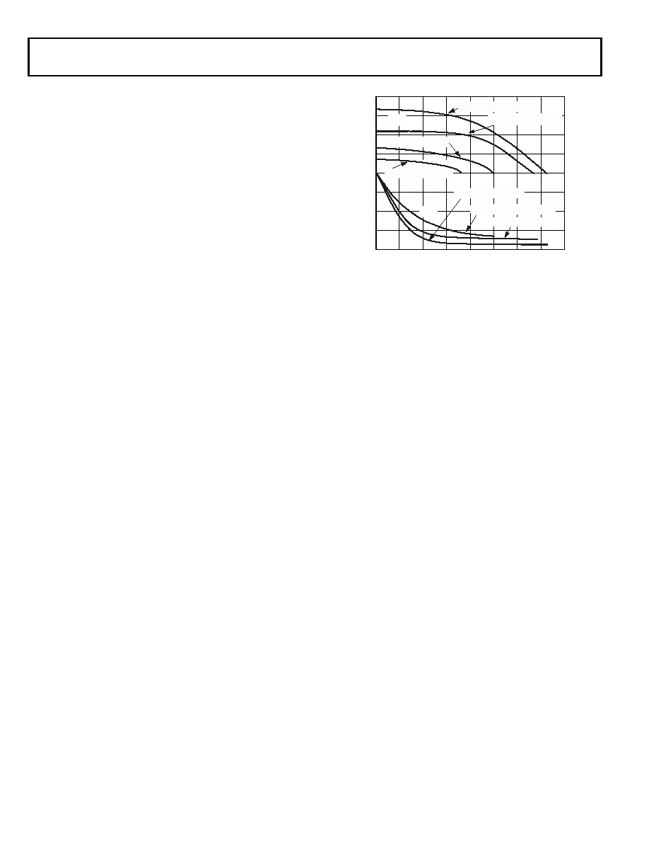
Output Drive Currents
Figure 21 shows typical I-V characteristics for the output driv-
ers on the ADSP-218xN series.The curves represent the current
drive capability of the output drivers as a function of
output voltage.
Figure 23 shows the typical power-down supply current.
Capacitive Loading
tics of the ADSP-218xN.
Figure 21. Typical Output Driver Characteristics
for VDDEXT at 3.6 V, 3.3 V, 2.5 V, and 1.8 V
V OL
SOURCE VOLTAGE – V
00.5
1.0
S
O
U
R
C
E
C
U
R
E
N
T
–
m
A
60
0
–20
–40
–60
40
20
VDDEXT =3.6V@ –40 C
VDDEXT =3.3V@ +25 C
VDDEXT = 1.8/2.5V @ +85 C
VDDEXT =2.5V @ +85 C
V DDEXT = 3.6 V @ –40 C
80
–80
1.5
2.0
2.5
3.0
3.5
4.0
VDDEXT = 1.8/2.5V @ +85 C
V
OH
VDDEXT =3.3V @ +25 C
VDDEXT =1.8V @ +85 C
相关PDF资料 |
PDF描述 |
|---|---|
| VI-2WF-CY-F3 | CONVERTER MOD DC/DC 72V 50W |
| RCM08DTBD-S189 | CONN EDGECARD 16POS R/A .156 SLD |
| VI-2WB-CY-F1 | CONVERTER MOD DC/DC 95V 50W |
| MIC3232YMM | IC LED DRVR HP CONS CURR 10-MSOP |
| 1130-561K-RC | CHOKE RF HI CURR 560UH 10% RAD |
相关代理商/技术参数 |
参数描述 |
|---|---|
| ADSP-2188NKSTZ-3202 | 制造商:AD 制造商全称:Analog Devices 功能描述:DSP Microcomputer |
| ADSP-2188N-WFA | 制造商:Analog Devices 功能描述: |
| ADSP-2189 | 制造商:AD 制造商全称:Analog Devices 功能描述:DSP Microcomputer |
| ADSP-2189M | 制造商:AD 制造商全称:Analog Devices 功能描述:DSP Microcomputer |
| ADSP-2189M_99 | 制造商:AD 制造商全称:Analog Devices 功能描述:DSP Microcomputer |
发布紧急采购,3分钟左右您将得到回复。