- 您现在的位置:买卖IC网 > PDF目录19382 > ADSP-2188NKSTZ-320 (Analog Devices Inc)IC DSP CONTROLLER 16BIT 100LQFP PDF资料下载
参数资料
| 型号: | ADSP-2188NKSTZ-320 |
| 厂商: | Analog Devices Inc |
| 文件页数: | 24/48页 |
| 文件大小: | 0K |
| 描述: | IC DSP CONTROLLER 16BIT 100LQFP |
| 标准包装: | 1 |
| 系列: | ADSP-21xx |
| 类型: | 定点 |
| 接口: | 主机接口,串行端口 |
| 时钟速率: | 80MHz |
| 非易失内存: | 外部 |
| 芯片上RAM: | 256kB |
| 电压 - 输入/输出: | 1.8V,2.5V,3.3V |
| 电压 - 核心: | 1.80V |
| 工作温度: | 0°C ~ 70°C |
| 安装类型: | 表面贴装 |
| 封装/外壳: | 100-LQFP |
| 供应商设备封装: | 100-LQFP(14x14) |
| 包装: | 托盘 |
第1页第2页第3页第4页第5页第6页第7页第8页第9页第10页第11页第12页第13页第14页第15页第16页第17页第18页第19页第20页第21页第22页第23页当前第24页第25页第26页第27页第28页第29页第30页第31页第32页第33页第34页第35页第36页第37页第38页第39页第40页第41页第42页第43页第44页第45页第46页第47页第48页
Rev. A
|
Page 30 of 48
|
August 2006
ADSP-218xN
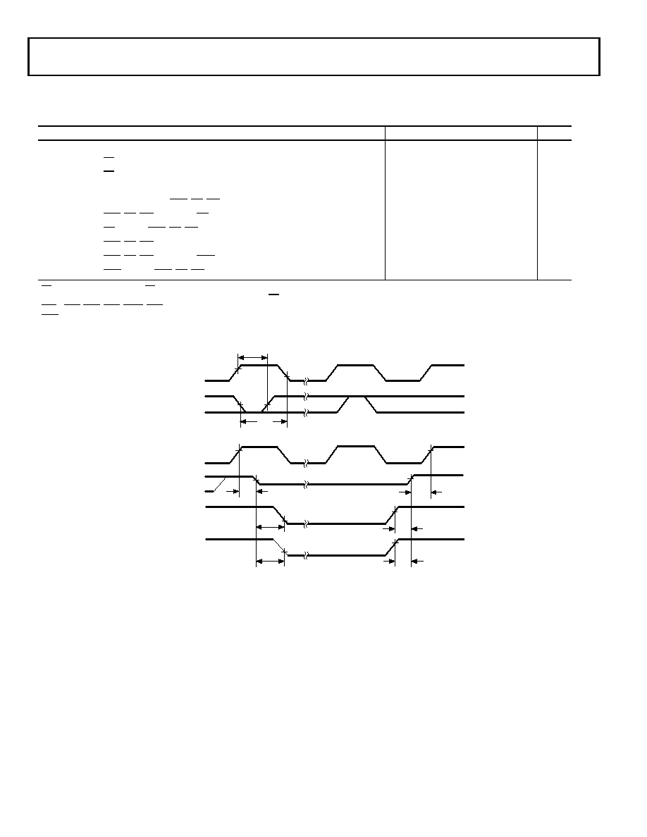
Bus Request–Bus Grant
Table 17. Bus Request–Bus Grant
Parameter
Min
Max
Unit
Timing Requirements:
tBH
BR Hold after CLKOUT High1
1 BR is an asynchronous signal. If BR meets the setup/hold requirements, it will be recognized during the current clock cycle; otherwise the signal will be recognized on
the following cycle. Refer to the ADSP-2100 Family User’s Manual for BR/BG cycle relationships.
0.25tCK + 2
ns
tBS
BR Setup before CLKOUT Low1
0.25tCK + 8
ns
Switching Characteristics:
tSD
CLKOUT High to xMS, RD, WR Disable
2
2 xMS = PMS, DMS, CMS, IOMS, BMS.
0.25tCK + 8
ns
tSDB
xMS, RD, WR Disable to BG Low
0
ns
tSE
BG High to xMS, RD, WR Enable
0
ns
tSEC
xMS, RD, WR Enable to CLKOUT High
0.25tCK – 3
ns
tSDBH
xMS, RD, WR Disable to BGH Low3
3 BGH is asserted when the bus is granted and the processor or BDMA requires control of the bus to continue.
0ns
tSEH
BGH High to xMS, RD, WR Enable3
0ns
Figure 28. Bus Request–Bus Grant
CLKOUT
tSD
tSDB
tSE
tSEC
t
SDBH
tSEH
tBS
BR
tBH
CLKOUT
PMS, DMS
BMS, RD
CMS, WR,
IOMS
BG
BGH
相关PDF资料 |
PDF描述 |
|---|---|
| VI-2WF-CY-F3 | CONVERTER MOD DC/DC 72V 50W |
| RCM08DTBD-S189 | CONN EDGECARD 16POS R/A .156 SLD |
| VI-2WB-CY-F1 | CONVERTER MOD DC/DC 95V 50W |
| MIC3232YMM | IC LED DRVR HP CONS CURR 10-MSOP |
| 1130-561K-RC | CHOKE RF HI CURR 560UH 10% RAD |
相关代理商/技术参数 |
参数描述 |
|---|---|
| ADSP-2188NKSTZ-3202 | 制造商:AD 制造商全称:Analog Devices 功能描述:DSP Microcomputer |
| ADSP-2188N-WFA | 制造商:Analog Devices 功能描述: |
| ADSP-2189 | 制造商:AD 制造商全称:Analog Devices 功能描述:DSP Microcomputer |
| ADSP-2189M | 制造商:AD 制造商全称:Analog Devices 功能描述:DSP Microcomputer |
| ADSP-2189M_99 | 制造商:AD 制造商全称:Analog Devices 功能描述:DSP Microcomputer |
发布紧急采购,3分钟左右您将得到回复。