- 您现在的位置:买卖IC网 > PDF目录19382 > ADSP-2188NKSTZ-320 (Analog Devices Inc)IC DSP CONTROLLER 16BIT 100LQFP PDF资料下载
参数资料
| 型号: | ADSP-2188NKSTZ-320 |
| 厂商: | Analog Devices Inc |
| 文件页数: | 4/48页 |
| 文件大小: | 0K |
| 描述: | IC DSP CONTROLLER 16BIT 100LQFP |
| 标准包装: | 1 |
| 系列: | ADSP-21xx |
| 类型: | 定点 |
| 接口: | 主机接口,串行端口 |
| 时钟速率: | 80MHz |
| 非易失内存: | 外部 |
| 芯片上RAM: | 256kB |
| 电压 - 输入/输出: | 1.8V,2.5V,3.3V |
| 电压 - 核心: | 1.80V |
| 工作温度: | 0°C ~ 70°C |
| 安装类型: | 表面贴装 |
| 封装/外壳: | 100-LQFP |
| 供应商设备封装: | 100-LQFP(14x14) |
| 包装: | 托盘 |
第1页第2页第3页当前第4页第5页第6页第7页第8页第9页第10页第11页第12页第13页第14页第15页第16页第17页第18页第19页第20页第21页第22页第23页第24页第25页第26页第27页第28页第29页第30页第31页第32页第33页第34页第35页第36页第37页第38页第39页第40页第41页第42页第43页第44页第45页第46页第47页第48页
Rev. A
|
Page 12 of 48
|
August 2006
ADSP-218xN
IOWAIT0–3 as shown in Figure 10, which in combination with
the wait state mode bit, specify up to 15 wait states to be auto-
matically generated for each of four regions. The wait states act
on address ranges, as shown in Table 6.
Note
: In Full Memory Mode, all 2048 locations of I/O space are
directly addressable. In Host Memory Mode, only address pin
A0 is available; therefore, additional logic is required externally
to achieve complete addressability of the 2048 I/O
space locations.
Composite Memory Select
ADSP-218xN series members have a programmable memory
select signal that is useful for generating memory select signals
for memories mapped to more than one space. The CMS signal
is generated to have the same timing as each of the individual
memory select signals (PMS, DMS, BMS, IOMS) but can com-
bine their functionality. Each bit in the CMSSEL register, when
set, causes the CMS signal to be asserted when the selected
memory select is asserted. For example, to use a 32K word
memory to act as both program and data memory, set the PMS
and DMS bits in the CMSSEL register and use the CMS pin to
drive the chip select of the memory, and use either DMS or PMS
as the additional address bit.
The CMS pin functions like the other memory select signals
with the same timing and bus request logic. A 1 in the enable bit
causes the assertion of the CMS signal at the same time as the
selected memory select signal. All enable bits default to 1 at
reset, except the BMS bit.
ble flag and composite control register and the system
control register.
Byte Memory Select
The ADSP-218xN’s BMS disable feature combined with the
CMS pin allows use of multiple memories in the byte memory
space. For example, an EPROM could be attached to the BMS
select, and a flash memory could be connected to CMS. Because
at reset BMS is enabled, the EPROM would be used for booting.
After booting, software could disable BMS and set the CMS sig-
nal to respond to BMS, enabling the flash memory.
Byte Memory
The byte memory space is a bidirectional, 8-bit-wide,
external memory space used to store programs and data. Byte
memory is accessed using the BDMA feature. The byte memory
space consists of 256 pages, each of which is 16K
8bits.
The byte memory space on the ADSP-218xN series supports
read and write operations as well as four different data formats.
The byte memory uses data bits 15–8 for data. The byte mem-
ory uses data bits 23–16 and address bits 13–0 to create a 22-bit
address. This allows up to a 4 megabit
8 (32 megabit) ROM
or RAM to be used without glue logic. All byte memory accesses
are timed by the BMWAIT register and the wait state mode bit.
Byte Memory DMA (BDMA, Full Memory Mode)
The byte memory DMA controller (Figure 13) allows loading
and storing of program instructions and data using the byte
memory space. The BDMA circuit is able to access the byte
memory space while the processor is operating normally and
steals only one DSP cycle per 8-, 16-, or 24-bit word transferred.
Table 6. Wait States
Address Range
Wait State Register
0x000–0x1FF
IOWAIT0 and Wait State Mode Select Bit
0x200–0x3FF
IOWAIT1 and Wait State Mode Select Bit
0x400–0x5FF
IOWAIT2 and Wait State Mode Select Bit
0x600–0x7FF
IOWAIT3 and Wait State Mode Select Bit
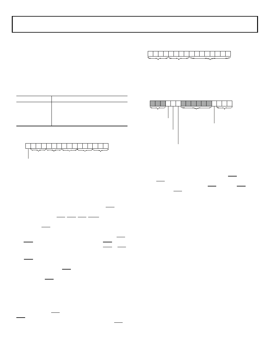
Figure 10. Wait State Control Register
In
ser
t W
ait
St
ate
Con
tro
l R
eg
ist
er
DWAIT
IOWAIT3
IOWAIT2
IOWAIT1
IOWAIT0
DM(0x3FFE)
WAIT STATE CONTROL
11
1
11
1
11
1 5 14 13 12 11 10
9
8
7
6
5
4
3
2
1
0
WAIT STATE MODE SELECT
0 = NORMAL MODE (PWAIT, DWAIT, IOWAIT0–3 = N WAIT STATES,
RANGING FROM 0 TO 7)
1 = 2N + 1 MODE (PWAIT, DWAIT, IOWAIT0–3 = 2N + 1 WAIT STATES,
RANGING FROM 0 TO 15)
Figure 11. Programmable Flag and Composite Control Register
Figure 12. System Control Register
BMW AIT
CM S S EL
0=D IS A BLE
CMS
1=E N AB LE
CMS
DM(0x3FE6)
PF TYPE
0= I N PUT
1= O U TP UT
( WH ER E B IT : 11 - IOM , 1 0 -B M, 9-DM , 8-P M )
1
0
1
00
0
15 14 13 12 11 10
9
8
7
6
5
4
3
2
1
0
PROGRAMMABLE FLAG AND COMPOSITE
SELECT CONTROL
RESERVED,ALW AY S
SE T TO 0
SP O RT0 E NABL E
0 = DIS ABL E
1= E NABL E
DM (0x3F FF)
S YSTEM CONTROL
S P ORT 1 E NABLE
0 = DIS ABLE
1 = ENABLE
S PO RT1 C ONF IGURE
0= FI,FO ,
IRQ0, IRQ1,SCLK
1= SPO RT1
DISABLE
BMS
0 = E NABL E
BMS
1= DIS AB LE
BMS
PWAIT
PROGRAM MEMOR Y
W AIT ST ATES
0
00
01
00
0
1
15 14 13 12 11 10
9
8
7
6
5
4
3
2
1
0
N OTE : RESERVED BITS ARE SHO WN O N A G RAY FIELD . THESE B ITS
SHOUL D ALW AYS BE WR ITTE N W ITH Z EROS .
RES ERV ED
SE T T O 0
相关PDF资料 |
PDF描述 |
|---|---|
| VI-2WF-CY-F3 | CONVERTER MOD DC/DC 72V 50W |
| RCM08DTBD-S189 | CONN EDGECARD 16POS R/A .156 SLD |
| VI-2WB-CY-F1 | CONVERTER MOD DC/DC 95V 50W |
| MIC3232YMM | IC LED DRVR HP CONS CURR 10-MSOP |
| 1130-561K-RC | CHOKE RF HI CURR 560UH 10% RAD |
相关代理商/技术参数 |
参数描述 |
|---|---|
| ADSP-2188NKSTZ-3202 | 制造商:AD 制造商全称:Analog Devices 功能描述:DSP Microcomputer |
| ADSP-2188N-WFA | 制造商:Analog Devices 功能描述: |
| ADSP-2189 | 制造商:AD 制造商全称:Analog Devices 功能描述:DSP Microcomputer |
| ADSP-2189M | 制造商:AD 制造商全称:Analog Devices 功能描述:DSP Microcomputer |
| ADSP-2189M_99 | 制造商:AD 制造商全称:Analog Devices 功能描述:DSP Microcomputer |
发布紧急采购,3分钟左右您将得到回复。