- 您现在的位置:买卖IC网 > PDF目录19468 > ADSP-2189MKSTZ-300 (Analog Devices Inc)IC DSP CONTROLLER 16BIT 100-LQFP PDF资料下载
参数资料
| 型号: | ADSP-2189MKSTZ-300 |
| 厂商: | Analog Devices Inc |
| 文件页数: | 1/32页 |
| 文件大小: | 0K |
| 描述: | IC DSP CONTROLLER 16BIT 100-LQFP |
| 标准包装: | 1 |
| 系列: | ADSP-21xx |
| 类型: | 定点 |
| 接口: | 主机接口,串行端口 |
| 时钟速率: | 75MHz |
| 非易失内存: | 外部 |
| 芯片上RAM: | 192kB |
| 电压 - 输入/输出: | 3.30V |
| 电压 - 核心: | 2.50V |
| 工作温度: | 0°C ~ 70°C |
| 安装类型: | 表面贴装 |
| 封装/外壳: | 100-LQFP |
| 供应商设备封装: | 100-LQFP(14x14) |
| 包装: | 托盘 |
| 其它名称: | ADSP-2189MKSTZ300 ADSP-2189MKSTZ300-ND |
当前第1页第2页第3页第4页第5页第6页第7页第8页第9页第10页第11页第12页第13页第14页第15页第16页第17页第18页第19页第20页第21页第22页第23页第24页第25页第26页第27页第28页第29页第30页第31页第32页
REV. A
Information furnished by Analog Devices is believed to be accurate and
reliable. However, no responsibility is assumed by Analog Devices for its
use, nor for any infringements of patents or other rights of third parties
which may result from its use. No license is granted by implication or
otherwise under any patent or patent rights of Analog Devices.
a
ADSP-2189M
One Technology Way, P.O. Box 9106, Norwood, MA 02062-9106, U.S.A.
Tel: 781/329-4700
World Wide Web Site: http://www.analog.com
Fax: 781/326-8703
Analog Devices, Inc., 2000
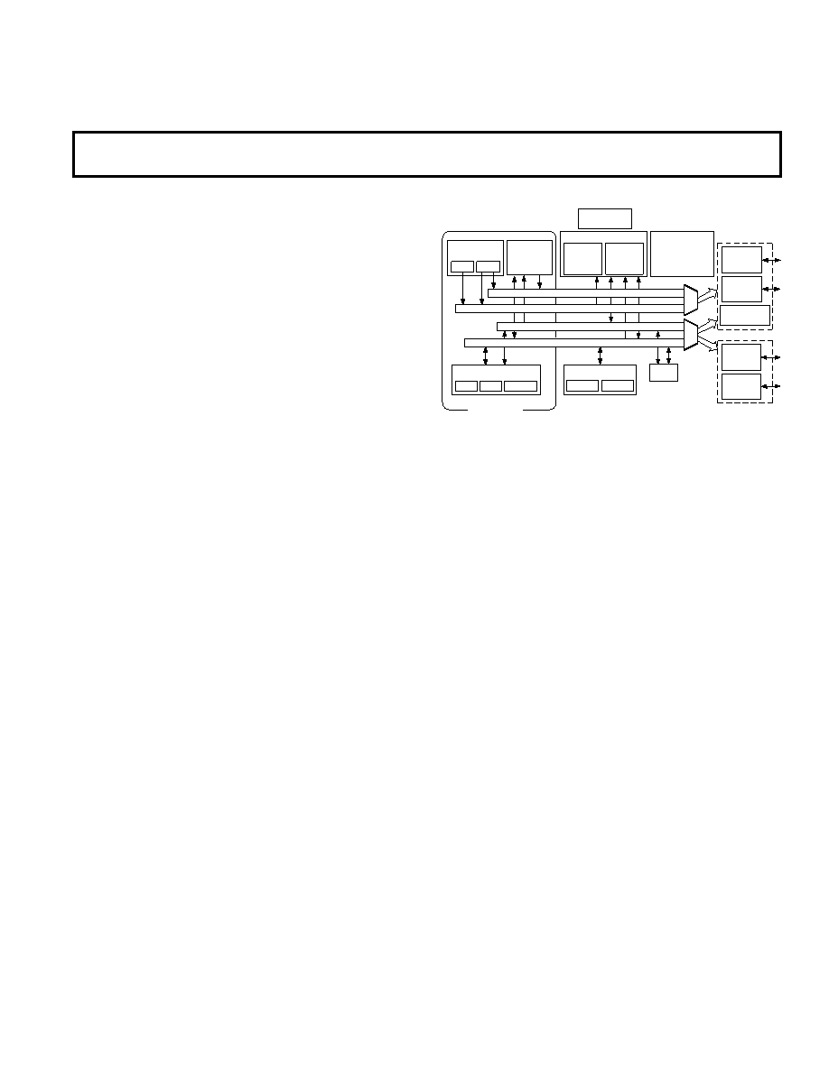
DSP Microcomputer
FUNCTIONAL BLOCK DIAGRAM
SERIAL PORTS
SPORT 1
SPORT 0
MEMORY
PROGRAMMABLE
I/O
AND
FLAGS
BYTE DMA
CONTROLLER
PROGRAM
MEMORY
32K
24 BIT
DATA
MEMORY
48K
16 BIT
TIMER
ADSP-2100 BASE
ARCHITECTURE
SHIFTER
MAC
ALU
ARITHMETIC UNITS
POWER-DOWN
CONTROL
PROGRAM
SEQUENCER
DAG 2
DAG 1
DATA ADDRESS
GENERATORS
PROGRAM MEMORY ADDRESS
DATA MEMORY ADDRESS
PROGRAM MEMORY DATA
DATA MEMORY DATA
EXTERNAL
DATA
BUS
EXTERNAL
ADDRESS
BUS
INTERNAL
DMA
PORT
EXTERNAL
DATA
BUS
OR
FULL MEMORY
MODE
HOST MODE
GENERAL DESCRIPTION
The ADSP-2189M is a single-chip microcomputer optimized
for digital signal processing (DSP) and other high speed nu-
meric processing applications.
The ADSP-2189M combines the ADSP-2100 family base archi-
tecture (three computational units, data address generators and
a program sequencer) with two serial ports, a 16-bit internal
DMA port, a byte DMA port, a programmable timer, Flag I/O,
extensive interrupt capabilities, and on-chip program and data
memory.
The ADSP-2189M integrates 192K bytes of on-chip memory
configured as 32K words (24-bit) of program RAM and 48K
words (16-bit) of data RAM. Power-down circuitry is also pro-
vided to meet the low power needs of battery operated portable
equipment. The ADSP-2189M is available in a 100-lead LQFP
package.
In addition, the ADSP-2189M supports new instructions, which
include bit manipulations—bit set, bit clear, bit toggle, bit test—
new ALU constants, new multiplication instruction (x squared),
biased rounding, result free ALU operations, I/O memory trans-
fers and global interrupt masking, for increased flexibility.
FEATURES
PERFORMANCE
13.3 ns Instruction Cycle Time @ 2.5 Volts (Internal),
75 MIPS Sustained Performance
Single-Cycle Instruction Execution
Single-Cycle Context Switch
3-Bus Architecture Allows Dual Operand Fetches in
Every Instruction Cycle
Multifunction Instructions
Power-Down Mode Featuring Low CMOS Standby
Power Dissipation with 200 CLKIN Cycle Recovery
from Power-Down Condition
Low Power Dissipation in Idle Mode
INTEGRATION
ADSP-2100 Family Code Compatible (Easy to Use Alge-
braic Syntax), with Instruction Set Extensions
192K Bytes of On-Chip RAM, Configured as 32K Words
On-Chip Program Memory RAM and 48K Words On-
Chip Data Memory RAM
Dual Purpose Program Memory for Both Instruction
and Data Storage
Independent ALU, Multiplier/Accumulator and Barrel
Shifter Computational Units
Two Independent Data Address Generators
Powerful Program Sequencer Provides Zero Overhead
Looping Conditional Instruction Execution
Programmable 16-Bit Interval Timer with Prescaler
100-Lead LQFP
SYSTEM INTERFACE
Flexible I/O Structure Allows 2.5 V or 3.3 V Operation;
All Inputs Tolerate Up to 3.6 V, Regardless of Mode
16-Bit Internal DMA Port for High Speed Access to On-
Chip Memory (Mode Selectable)
4 MByte Memory Interface for Storage of Data Tables
and Program Overlays (Mode Selectable)
8-Bit DMA to Byte Memory for Transparent Program
and Data Memory Transfers (Mode Selectable)
I/O Memory Interface with 2048 Locations Supports
Parallel Peripherals (Mode Selectable)
Programmable Memory Strobe and Separate I/O
Memory Space Permits “Glueless” System Design
Programmable Wait-State Generation
Two Double-Buffered Serial Ports with Companding
Hardware and Automatic Data Buffering
Automatic Booting of On-Chip Program Memory from
Byte-Wide External Memory, e.g., EPROM, or
Through Internal DMA Port
Six External Interrupts
13 Programmable Flag Pins Provide Flexible System
Signaling
UART Emulation through Software SPORT Reconfiguration
ICE-Port Emulator Interface Supports Debugging in
Final Systems
ICE-Port is a trademark of Analog Devices, Inc.
相关PDF资料 |
PDF描述 |
|---|---|
| VI-B1N-CX-B1 | CONVERTER MOD DC/DC 18.5V 75W |
| VE-21N-CY-F2 | CONVERTER MOD DC/DC 18.5V 50W |
| ADSP-21369KSWZ-5A | IC DSP 32BIT 366MHZ 208LQFP |
| TAP106M035BRW | CAP TANT 10UF 35V 20% RADIAL |
| XC2C384-10FGG324C | IC CR-II CPLD 384MCELL 324-FBGA |
相关代理商/技术参数 |
参数描述 |
|---|---|
| ADSP-2189MKSTZ-300 | 制造商:Analog Devices 功能描述:IC 16-BIT MICROCOMPUTER |
| ADSP-2189N | 制造商:AD 制造商全称:Analog Devices 功能描述:DSP Microcomputer |
| ADSP-2189NBCA-320 | 功能描述:IC DSP 16BIT 80MHZ 144CSPBGA RoHS:否 类别:集成电路 (IC) >> 嵌入式 - DSP(数字式信号处理器) 系列:ADSP-21xx 标准包装:2 系列:StarCore 类型:SC140 内核 接口:DSI,以太网,RS-232 时钟速率:400MHz 非易失内存:外部 芯片上RAM:1.436MB 电压 - 输入/输出:3.30V 电压 - 核心:1.20V 工作温度:-40°C ~ 105°C 安装类型:表面贴装 封装/外壳:431-BFBGA,FCBGA 供应商设备封装:431-FCPBGA(20x20) 包装:托盘 |
| ADSP-2189NBCAZ-320 | 功能描述:IC DSP 16BIT 80MHZ 144CSPBGA RoHS:是 类别:集成电路 (IC) >> 嵌入式 - DSP(数字式信号处理器) 系列:ADSP-21xx 标准包装:2 系列:StarCore 类型:SC140 内核 接口:DSI,以太网,RS-232 时钟速率:400MHz 非易失内存:外部 芯片上RAM:1.436MB 电压 - 输入/输出:3.30V 电压 - 核心:1.20V 工作温度:-40°C ~ 105°C 安装类型:表面贴装 封装/外壳:431-BFBGA,FCBGA 供应商设备封装:431-FCPBGA(20x20) 包装:托盘 |
| ADSP-2189NBCAZ-3202 | 制造商:AD 制造商全称:Analog Devices 功能描述:DSP Microcomputer |
发布紧急采购,3分钟左右您将得到回复。