- 您现在的位置:买卖IC网 > PDF目录19468 > ADSP-2189MKSTZ-300 (Analog Devices Inc)IC DSP CONTROLLER 16BIT 100-LQFP PDF资料下载
参数资料
| 型号: | ADSP-2189MKSTZ-300 |
| 厂商: | Analog Devices Inc |
| 文件页数: | 2/32页 |
| 文件大小: | 0K |
| 描述: | IC DSP CONTROLLER 16BIT 100-LQFP |
| 标准包装: | 1 |
| 系列: | ADSP-21xx |
| 类型: | 定点 |
| 接口: | 主机接口,串行端口 |
| 时钟速率: | 75MHz |
| 非易失内存: | 外部 |
| 芯片上RAM: | 192kB |
| 电压 - 输入/输出: | 3.30V |
| 电压 - 核心: | 2.50V |
| 工作温度: | 0°C ~ 70°C |
| 安装类型: | 表面贴装 |
| 封装/外壳: | 100-LQFP |
| 供应商设备封装: | 100-LQFP(14x14) |
| 包装: | 托盘 |
| 其它名称: | ADSP-2189MKSTZ300 ADSP-2189MKSTZ300-ND |
第1页当前第2页第3页第4页第5页第6页第7页第8页第9页第10页第11页第12页第13页第14页第15页第16页第17页第18页第19页第20页第21页第22页第23页第24页第25页第26页第27页第28页第29页第30页第31页第32页
REV. A
ADSP-2189M
–10–
Byte Memory
The byte memory space is a bidirectional, 8-bit-wide, external
memory space used to store programs and data. Byte memory is
accessed using the BDMA feature. The byte memory space
consists of 256 pages, each of which is 16K
× 8.
The byte memory space on the ADSP-2189M supports read
and write operations as well as four different data formats. The
byte memory uses data bits 15:8 for data. The byte memory
uses data bits 23:16 and address bits 13:0 to create a 22-bit
address. This allows up to a 4 meg
× 8 (32 megabit) ROM or
RAM to be used without glue logic. All byte memory accesses
are timed by the BMWAIT register and the wait-state mode bit.
Byte Memory DMA (BDMA, Full Memory Mode)
The Byte memory DMA controller allows loading and storing of
program instructions and data using the byte memory space.
The BDMA circuit is able to access the byte memory space
while the processor is operating normally and steals only one
DSP cycle per 8-, 16- or 24-bit word transferred.
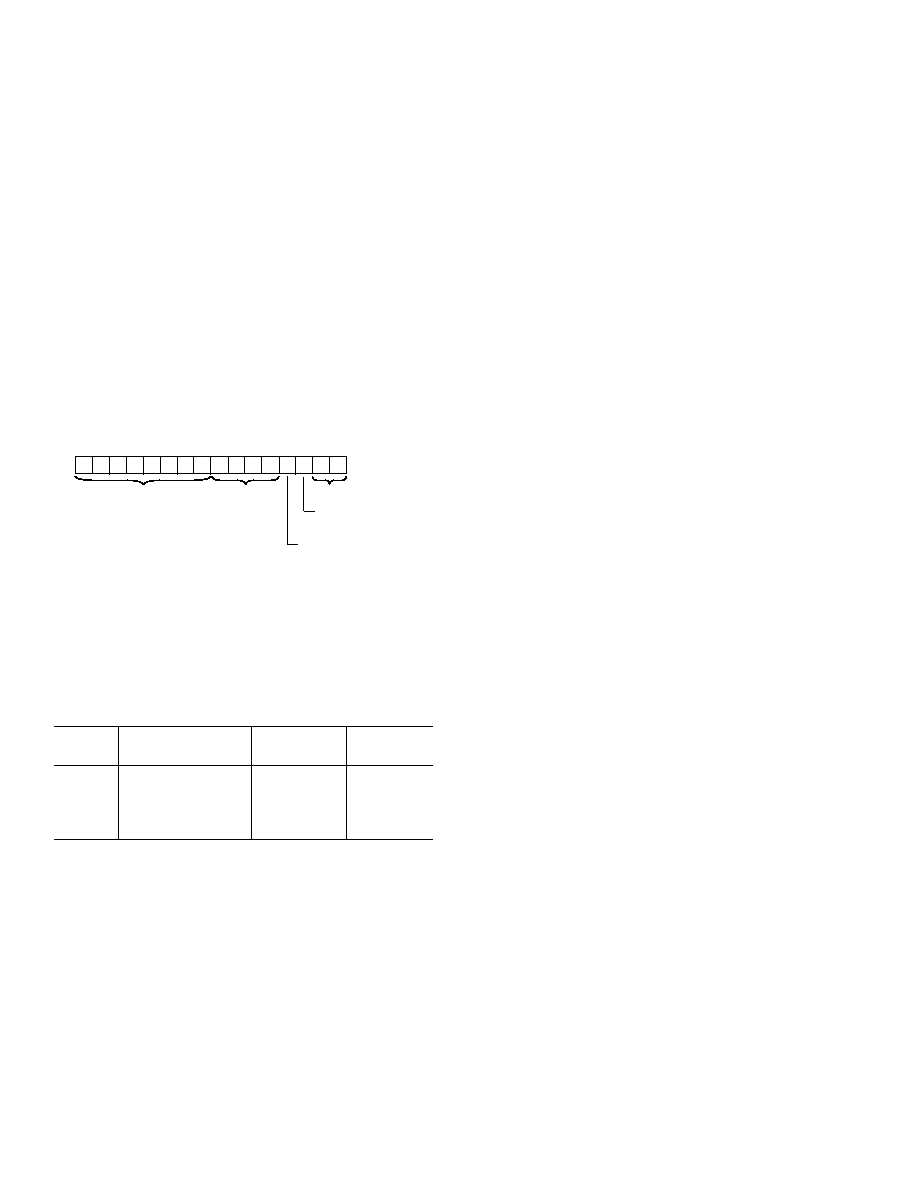
BDMA CONTROL
BMPAGE
BDMA
OVERLAY
BITS
BTYPE
BDIR
0 = LOAD FROM BM
1 = STORE TO BM
BCR
0 = RUN DURING BDMA
1 = HALT DURING BDMA
00
0
00
000
0
1
0
15 14 13 12 11 10
9
8
7
6
5
43210
DM (0 3FE3)
Figure 9. BDMA Control Register
The BDMA circuit supports four different data formats which
are selected by the BTYPE register field. The appropriate num-
ber of 8-bit accesses are done from the byte memory space to
build the word size selected. Table VI shows the data formats
supported by the BDMA circuit.
Table VI. Data Formats
Internal
BTYPE
Memory Space
Word Size
Alignment
00
Program Memory
24
Full Word
01
Data Memory
16
Full Word
10
Data Memory
8
MSBs
11
Data Memory
8
LSBs
Unused bits in the 8-bit data memory formats are filled with 0s.
The BIAD register field is used to specify the starting address
for the on-chip memory involved with the transfer. The 14-bit
BEAD register specifies the starting address for the external byte
memory space. The 8-bit BMPAGE register specifies the start-
ing page for the external byte memory space. The BDIR register
field selects the direction of the transfer. Finally, the 14-bit
BWCOUNT register specifies the number of DSP words to
transfer and initiates the BDMA circuit transfers.
BDMA accesses can cross page boundaries during sequential
addressing. A BDMA interrupt is generated on the completion
of the number of transfers specified by the BWCOUNT register.
The BWCOUNT register is updated after each transfer so it can
be used to check the status of the transfers. When it reaches
zero, the transfers have finished and a BDMA interrupt is gener-
ated. The BMPAGE and BEAD registers must not be accessed
by the DSP during BDMA operations.
The source or destination of a BDMA transfer will always be
on-chip program or data memory.
When the BWCOUNT register is written with a nonzero value
the BDMA circuit starts executing byte memory accesses with
wait-states set by BMWAIT. These accesses continue until the
count reaches zero. When enough accesses have occurred to
create a destination word, it is transferred to or from on-chip
memory. The transfer takes one DSP cycle. DSP accesses to
external memory have priority over BDMA byte memory
accesses.
The BDMA Context Reset bit (BCR) controls whether the
processor is held off while the BDMA accesses are occurring.
Setting the BCR bit to 0 allows the processor to continue opera-
tions. Setting the BCR bit to 1 causes the processor to stop
execution while the BDMA accesses are occurring, to clear the
context of the processor, and start execution at address 0 when
the BDMA accesses have completed.
The BDMA overlay bits specify the OVLAY memory blocks to
be accessed for internal memory.
The BMWAIT field, which has four bits on ADSP-2189M,
allows selection of up to 15 wait-states for BDMA transfers.
Internal Memory DMA Port (IDMA Port; Host Memory
Mode)
The IDMA Port provides an efficient means of communication
between a host system and the ADSP-2189M. The port is used
to access the on-chip program memory and data memory of the
DSP with only one DSP cycle per word overhead. The IDMA
port cannot, however, be used to write to the DSP’s memory-
mapped control registers. A typical IDMA transfer process is
described as follows:
1. Host starts IDMA transfer.
2. Host checks
IACK control line to see if the DSP is busy.
3. Host uses
IS and IAL control lines to latch either the DMA
starting address (IDMAA) or the PM/DM OVLAY selection
into the DSP’s IDMA control registers. If Bit 15 = 1, the
value of bits 7:0 represent the IDMA overlay: Bits 14:8 must
be set to 0. If Bit 15 = 0, the value of bits 13:0 represent the
starting address of internal memory to be accessed and Bit 14
reflects PM or DM for access.
4. Host uses
IS and IRD (or IWR) to read (or write) DSP inter-
nal memory (PM or DM).
5. Host checks
IACK line to see if the DSP has completed the
previous IDMA operation.
6. Host ends IDMA transfer.
相关PDF资料 |
PDF描述 |
|---|---|
| VI-B1N-CX-B1 | CONVERTER MOD DC/DC 18.5V 75W |
| VE-21N-CY-F2 | CONVERTER MOD DC/DC 18.5V 50W |
| ADSP-21369KSWZ-5A | IC DSP 32BIT 366MHZ 208LQFP |
| TAP106M035BRW | CAP TANT 10UF 35V 20% RADIAL |
| XC2C384-10FGG324C | IC CR-II CPLD 384MCELL 324-FBGA |
相关代理商/技术参数 |
参数描述 |
|---|---|
| ADSP-2189MKSTZ-300 | 制造商:Analog Devices 功能描述:IC 16-BIT MICROCOMPUTER |
| ADSP-2189N | 制造商:AD 制造商全称:Analog Devices 功能描述:DSP Microcomputer |
| ADSP-2189NBCA-320 | 功能描述:IC DSP 16BIT 80MHZ 144CSPBGA RoHS:否 类别:集成电路 (IC) >> 嵌入式 - DSP(数字式信号处理器) 系列:ADSP-21xx 标准包装:2 系列:StarCore 类型:SC140 内核 接口:DSI,以太网,RS-232 时钟速率:400MHz 非易失内存:外部 芯片上RAM:1.436MB 电压 - 输入/输出:3.30V 电压 - 核心:1.20V 工作温度:-40°C ~ 105°C 安装类型:表面贴装 封装/外壳:431-BFBGA,FCBGA 供应商设备封装:431-FCPBGA(20x20) 包装:托盘 |
| ADSP-2189NBCAZ-320 | 功能描述:IC DSP 16BIT 80MHZ 144CSPBGA RoHS:是 类别:集成电路 (IC) >> 嵌入式 - DSP(数字式信号处理器) 系列:ADSP-21xx 标准包装:2 系列:StarCore 类型:SC140 内核 接口:DSI,以太网,RS-232 时钟速率:400MHz 非易失内存:外部 芯片上RAM:1.436MB 电压 - 输入/输出:3.30V 电压 - 核心:1.20V 工作温度:-40°C ~ 105°C 安装类型:表面贴装 封装/外壳:431-BFBGA,FCBGA 供应商设备封装:431-FCPBGA(20x20) 包装:托盘 |
| ADSP-2189NBCAZ-3202 | 制造商:AD 制造商全称:Analog Devices 功能描述:DSP Microcomputer |
发布紧急采购,3分钟左右您将得到回复。