- 您现在的位置:买卖IC网 > PDF目录19468 > ADSP-2189MKSTZ-300 (Analog Devices Inc)IC DSP CONTROLLER 16BIT 100-LQFP PDF资料下载
参数资料
| 型号: | ADSP-2189MKSTZ-300 |
| 厂商: | Analog Devices Inc |
| 文件页数: | 10/32页 |
| 文件大小: | 0K |
| 描述: | IC DSP CONTROLLER 16BIT 100-LQFP |
| 标准包装: | 1 |
| 系列: | ADSP-21xx |
| 类型: | 定点 |
| 接口: | 主机接口,串行端口 |
| 时钟速率: | 75MHz |
| 非易失内存: | 外部 |
| 芯片上RAM: | 192kB |
| 电压 - 输入/输出: | 3.30V |
| 电压 - 核心: | 2.50V |
| 工作温度: | 0°C ~ 70°C |
| 安装类型: | 表面贴装 |
| 封装/外壳: | 100-LQFP |
| 供应商设备封装: | 100-LQFP(14x14) |
| 包装: | 托盘 |
| 其它名称: | ADSP-2189MKSTZ300 ADSP-2189MKSTZ300-ND |
第1页第2页第3页第4页第5页第6页第7页第8页第9页当前第10页第11页第12页第13页第14页第15页第16页第17页第18页第19页第20页第21页第22页第23页第24页第25页第26页第27页第28页第29页第30页第31页第32页
REV. A
ADSP-2189M
–18–
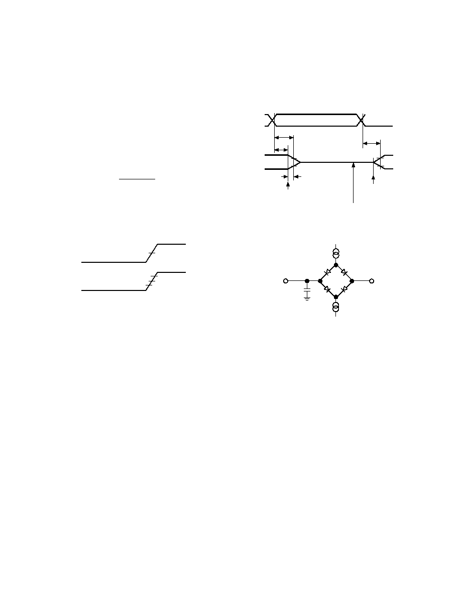
TEST CONDITIONS
Output Disable Time
Output pins are considered to be disabled when they have
stopped driving and started a transition from the measured
output high or low voltage to a high impedance state. The out-
put disable time (tDIS) is the difference of tMEASURED and tDECAY,
as shown in the Output Enable/Disable diagram. The time is the
interval from when a reference signal reaches a high or low
voltage level to when the output voltages have changed by 0.5 V
from the measured output high or low voltage.
The decay time, tDECAY, is dependent on the capacitive load,
CL, and the current load, iL, on the output pin. It can be ap-
proximated by the following equation:
t
CV
i
DECAY
L
=
× 05
.
from which
tDIS = tMEASURED – tDECAY
is calculated. If multiple pins (such as the data bus) are disabled,
the measurement value is that of the last pin to stop driving.
1.5V
OUTPUT
INPUT
1.5V
2.0V
0.8V
Figure 19. Voltage Reference Levels for AC Measurements
(Except Output Enable/Disable)
Output Enable Time
Output pins are considered to be enabled when they have made
a transition from a high impedance state to when they start
driving. The output enable time (tENA) is the interval from when
a reference signal reaches a high or low voltage level to when the
output has reached a specified high or low trip point, as shown
in the Output Enable/Disable diagram. If multiple pins (such as
the data bus) are enabled, the measurement value is that of the
first pin to start driving.
2.0V
1.0V
tENA
REFERENCE
SIGNAL
OUTPUT
tDECAY
VOH
(MEASURED)
OUTPUT STOPS
DRIVING
OUTPUT
STARTS
DRIVING
tDIS
tMEASURED
VOL
(MEASURED)
VOH (MEASURED) – 0.5V
VOL (MEASURED) +0.5V
HIGH-IMPEDANCE STATE. TEST CONDITIONS CAUSE
THIS VOLTAGE LEVEL TO BE APPROXIMATELY 1.5V.
VOH
(MEASURED)
VOL
(MEASURED)
Figure 20. Output Enable/Disable
TO
OUTPUT
PIN
50pF
+1.5V
IOH
IOL
Figure 21. Equivalent Device Loading for AC Measure-
ments (Including All Fixtures)
相关PDF资料 |
PDF描述 |
|---|---|
| VI-B1N-CX-B1 | CONVERTER MOD DC/DC 18.5V 75W |
| VE-21N-CY-F2 | CONVERTER MOD DC/DC 18.5V 50W |
| ADSP-21369KSWZ-5A | IC DSP 32BIT 366MHZ 208LQFP |
| TAP106M035BRW | CAP TANT 10UF 35V 20% RADIAL |
| XC2C384-10FGG324C | IC CR-II CPLD 384MCELL 324-FBGA |
相关代理商/技术参数 |
参数描述 |
|---|---|
| ADSP-2189MKSTZ-300 | 制造商:Analog Devices 功能描述:IC 16-BIT MICROCOMPUTER |
| ADSP-2189N | 制造商:AD 制造商全称:Analog Devices 功能描述:DSP Microcomputer |
| ADSP-2189NBCA-320 | 功能描述:IC DSP 16BIT 80MHZ 144CSPBGA RoHS:否 类别:集成电路 (IC) >> 嵌入式 - DSP(数字式信号处理器) 系列:ADSP-21xx 标准包装:2 系列:StarCore 类型:SC140 内核 接口:DSI,以太网,RS-232 时钟速率:400MHz 非易失内存:外部 芯片上RAM:1.436MB 电压 - 输入/输出:3.30V 电压 - 核心:1.20V 工作温度:-40°C ~ 105°C 安装类型:表面贴装 封装/外壳:431-BFBGA,FCBGA 供应商设备封装:431-FCPBGA(20x20) 包装:托盘 |
| ADSP-2189NBCAZ-320 | 功能描述:IC DSP 16BIT 80MHZ 144CSPBGA RoHS:是 类别:集成电路 (IC) >> 嵌入式 - DSP(数字式信号处理器) 系列:ADSP-21xx 标准包装:2 系列:StarCore 类型:SC140 内核 接口:DSI,以太网,RS-232 时钟速率:400MHz 非易失内存:外部 芯片上RAM:1.436MB 电压 - 输入/输出:3.30V 电压 - 核心:1.20V 工作温度:-40°C ~ 105°C 安装类型:表面贴装 封装/外壳:431-BFBGA,FCBGA 供应商设备封装:431-FCPBGA(20x20) 包装:托盘 |
| ADSP-2189NBCAZ-3202 | 制造商:AD 制造商全称:Analog Devices 功能描述:DSP Microcomputer |
发布紧急采购,3分钟左右您将得到回复。