- 您现在的位置:买卖IC网 > PDF目录19468 > ADSP-2189MKSTZ-300 (Analog Devices Inc)IC DSP CONTROLLER 16BIT 100-LQFP PDF资料下载
参数资料
| 型号: | ADSP-2189MKSTZ-300 |
| 厂商: | Analog Devices Inc |
| 文件页数: | 32/32页 |
| 文件大小: | 0K |
| 描述: | IC DSP CONTROLLER 16BIT 100-LQFP |
| 标准包装: | 1 |
| 系列: | ADSP-21xx |
| 类型: | 定点 |
| 接口: | 主机接口,串行端口 |
| 时钟速率: | 75MHz |
| 非易失内存: | 外部 |
| 芯片上RAM: | 192kB |
| 电压 - 输入/输出: | 3.30V |
| 电压 - 核心: | 2.50V |
| 工作温度: | 0°C ~ 70°C |
| 安装类型: | 表面贴装 |
| 封装/外壳: | 100-LQFP |
| 供应商设备封装: | 100-LQFP(14x14) |
| 包装: | 托盘 |
| 其它名称: | ADSP-2189MKSTZ300 ADSP-2189MKSTZ300-ND |
第1页第2页第3页第4页第5页第6页第7页第8页第9页第10页第11页第12页第13页第14页第15页第16页第17页第18页第19页第20页第21页第22页第23页第24页第25页第26页第27页第28页第29页第30页第31页当前第32页
REV. A
ADSP-2189M
–9–
Data Memory, Host Mode allows access to all internal
memory. External overlay access is limited by a single external
address line (A0).
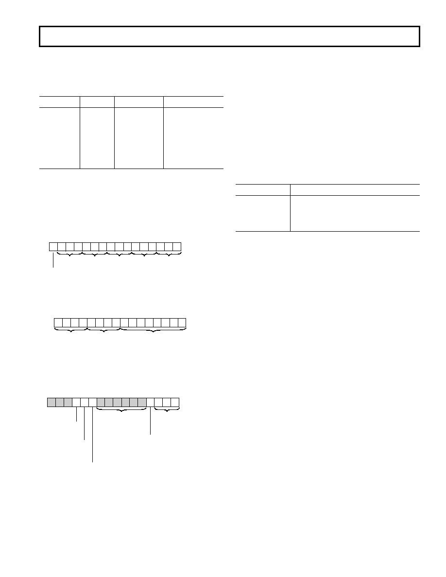
Table IV. DMOVLAY Bits
PMOVLAY
Memory
A13
A12:0
0, 4, 5, 6, 7
Internal
Not Applicable Not Applicable
1
External
0
13 LSBs of Address
Overlay 1
Between 0x2000
and 0x3FFF
2
External
1
13 LSBs of Address
Overlay 2
Between 0x2000
and 0x3FFF
Memory Mapped Registers (New to the ADSP-2189M)
The ADSP-2189M has three memory mapped registers that
differ from other ADSP-21xx Family DSPs. The slight modifi-
cations to these registers (Wait-State Control, Programmable
Flag and Composite Select Control and System Control) pro-
vide the ADSP-2189M’s wait-state and
BMS control features.
DWAIT
IOWAIT3
IOWAIT2
IOWAIT1
IOWAIT0
DM(0x3FFE)
WAIT STATE MODE SELECT (ADSP-2189M)
0 = NORMAL MODE (DWAIT, IOWAIT0-3 = N WAIT STATES, RANGING FROM 0 TO 7)
1 = 2N+1 MODE (DWAIT, IOWAIT0-3 = N WAIT STATES, RANGING FROM 0 TO 15)
WAIT-STATE CONTROL
11
1
11
111
1
15 14 13 12 11 10
9
8
7
6
5
43210
Figure 6. Wait-State Control Register (ADSP-2189M)
BMWAIT
(BIT-15, ADSP-2189M)
CMSSEL
0 = DISABLE CMS
1 = ENABLE CMS
DM(0x3FE6)
PROGRAMMABLE FLAG & COMPOSITE SELECT CONTROL
PFTYPE
0 = INPUT
1 = OUTPUT
(WHERE BIT: 11-IOM, 10BM, 9-DM, 8-PM)
11
1
11
111
1
15 14 13 12 11 10
9
8
7
6
5
43210
Figure 7. Programmable Flag and Composite Select Con-
trol Register
RESERVED, ALWAYS = 0
(ADSP-2189M)
SPORT0 ENABLE
0 = DISABLE
1 = ENABLE
DM(0x3FFF)
SYSTEM CONTROL
SPORT1 ENABLE
0 = DISABLE
1 = ENABLE
SPORT1 CONFIGURE
0 = FI, FO,
IRQ0, IRQ1, SCLK
1 = SPORT1
DISABLE
BMS (ADSP-2189M)
0 = ENABLE
BMS
1 = DISABLE
BMS, EXCEPT WHEN MEMORY
STROBES ARE THREE-STATED
PWAIT
PROGRAM MEMORY
WAIT STATES
00
0
1
00
000
0
1
15 14 13 12 11 10
9
8
7
6
5
43210
Figure 8. System Control Register
I/O Space (Full Memory Mode)
The ADSP-2189M supports an additional external memory
space called I/O space. This space is designed to support simple
connections to peripherals (such as data converters and external
registers) or to bus interface ASIC data registers. I/O space
supports 2048 locations of 16-bit-wide data. The lower eleven
bits of the external address bus are used; the upper three bits are
undefined. Two instructions were added to the core ADSP-2100
Family instruction set to read from and write to I/O memory
space. The I/O space also has four dedicated three-bit wait-state
registers, IOWAIT0–3, which, in combination with the wait-
state mode bit, specify up to 15 wait-states to be automatically
generated for each of four regions. The wait-states act on ad-
dress ranges as shown in Table V.
Table V. Wait-States
Address Range
Wait-State Register
0x000–0x1FF
IOWAIT0 and Wait-State Mode Select Bit
0x200–0x3FF
IOWAIT1 and Wait-State Mode Select Bit
0x400–0x5FF
IOWAIT2 and Wait-State Mode Select Bit
0x600–0x7FF
IOWAIT3 and Wait-State Mode Select Bit
Composite Memory Select (
CMS)
The ADSP-2189M has a programmable memory select signal
that is useful for generating memory select signals for memories
mapped to more than one space. The
CMS signal is generated
to have the same timing as each of the individual memory
select signals (
PMS, DMS, BMS, IOMS) but can combine
their functionality.
When set, each bit in the CMSSEL register causes the
CMS
signal to be asserted when the selected memory select is as-
serted. For example, to use a 32K word memory to act as both
program and data memory, set the
PMS and DMS bits in the
CMSSEL register and use the
CMS pin to drive the chip select
of the memory, and use either
DMS or PMS as the additional
address bit.
The
CMS pin functions like the other memory select signals,
with the same timing and bus request logic. A 1 in the enable bit
causes the assertion of the
CMS signal at the same time as the
selected memory select signal. All enable bits default to 1 at
reset, except the
BMS bit.
Byte Memory Select (
BMS)
The ADSP-2189M’s
BMS disable feature combined with the
CMS pin lets you use multiple memories in the byte memory
space. For example, an EPROM could be attached to the
BMS
select, and an SRAM could be connected to
CMS. Because
BMS is enabled at reset, the EPROM would be used for boot-
ing. After booting, software could disable
BMS and set the
CMS signal to respond to BMS, enabling the SRAM.
相关PDF资料 |
PDF描述 |
|---|---|
| VI-B1N-CX-B1 | CONVERTER MOD DC/DC 18.5V 75W |
| VE-21N-CY-F2 | CONVERTER MOD DC/DC 18.5V 50W |
| ADSP-21369KSWZ-5A | IC DSP 32BIT 366MHZ 208LQFP |
| TAP106M035BRW | CAP TANT 10UF 35V 20% RADIAL |
| XC2C384-10FGG324C | IC CR-II CPLD 384MCELL 324-FBGA |
相关代理商/技术参数 |
参数描述 |
|---|---|
| ADSP-2189MKSTZ-300 | 制造商:Analog Devices 功能描述:IC 16-BIT MICROCOMPUTER |
| ADSP-2189N | 制造商:AD 制造商全称:Analog Devices 功能描述:DSP Microcomputer |
| ADSP-2189NBCA-320 | 功能描述:IC DSP 16BIT 80MHZ 144CSPBGA RoHS:否 类别:集成电路 (IC) >> 嵌入式 - DSP(数字式信号处理器) 系列:ADSP-21xx 标准包装:2 系列:StarCore 类型:SC140 内核 接口:DSI,以太网,RS-232 时钟速率:400MHz 非易失内存:外部 芯片上RAM:1.436MB 电压 - 输入/输出:3.30V 电压 - 核心:1.20V 工作温度:-40°C ~ 105°C 安装类型:表面贴装 封装/外壳:431-BFBGA,FCBGA 供应商设备封装:431-FCPBGA(20x20) 包装:托盘 |
| ADSP-2189NBCAZ-320 | 功能描述:IC DSP 16BIT 80MHZ 144CSPBGA RoHS:是 类别:集成电路 (IC) >> 嵌入式 - DSP(数字式信号处理器) 系列:ADSP-21xx 标准包装:2 系列:StarCore 类型:SC140 内核 接口:DSI,以太网,RS-232 时钟速率:400MHz 非易失内存:外部 芯片上RAM:1.436MB 电压 - 输入/输出:3.30V 电压 - 核心:1.20V 工作温度:-40°C ~ 105°C 安装类型:表面贴装 封装/外壳:431-BFBGA,FCBGA 供应商设备封装:431-FCPBGA(20x20) 包装:托盘 |
| ADSP-2189NBCAZ-3202 | 制造商:AD 制造商全称:Analog Devices 功能描述:DSP Microcomputer |
发布紧急采购,3分钟左右您将得到回复。