- 您现在的位置:买卖IC网 > PDF目录19468 > ADSP-2189MKSTZ-300 (Analog Devices Inc)IC DSP CONTROLLER 16BIT 100-LQFP PDF资料下载
参数资料
| 型号: | ADSP-2189MKSTZ-300 |
| 厂商: | Analog Devices Inc |
| 文件页数: | 4/32页 |
| 文件大小: | 0K |
| 描述: | IC DSP CONTROLLER 16BIT 100-LQFP |
| 标准包装: | 1 |
| 系列: | ADSP-21xx |
| 类型: | 定点 |
| 接口: | 主机接口,串行端口 |
| 时钟速率: | 75MHz |
| 非易失内存: | 外部 |
| 芯片上RAM: | 192kB |
| 电压 - 输入/输出: | 3.30V |
| 电压 - 核心: | 2.50V |
| 工作温度: | 0°C ~ 70°C |
| 安装类型: | 表面贴装 |
| 封装/外壳: | 100-LQFP |
| 供应商设备封装: | 100-LQFP(14x14) |
| 包装: | 托盘 |
| 其它名称: | ADSP-2189MKSTZ300 ADSP-2189MKSTZ300-ND |
第1页第2页第3页当前第4页第5页第6页第7页第8页第9页第10页第11页第12页第13页第14页第15页第16页第17页第18页第19页第20页第21页第22页第23页第24页第25页第26页第27页第28页第29页第30页第31页第32页
REV. A
ADSP-2189M
–12–
Bus Request and Bus Grant
The ADSP-2189M can relinquish control of the data and ad-
dress buses to an external device. When the external device
requires access to memory, it asserts the bus request (
BR) sig-
nal. If the ADSP-2189M is not performing an external memory
access, it responds to the active
BR input in the following pro-
cessor cycle by:
Three-stating the data and address buses and the
PMS,
DMS, BMS, CMS, IOMS, RD, WR output drivers,
Asserting the bus grant (
BG) signal, and
Halting program execution.
If Go Mode is enabled, the ADSP-2189M will not halt program
execution until it encounters an instruction that requires an
external memory access.
If the ADSP-2189M is performing an external memory access
when the external device asserts the
BR signal, it will not three-
state the memory interfaces or assert the
BG signal until the
processor cycle after the access completes. The instruction does
not need to be completed when the bus is granted. If a single
instruction requires two external memory accesses, the bus will
be granted between the two accesses.
When the
BR signal is released, the processor releases the BG
signal, reenables the output drivers and continues program
execution from the point at which it stopped.
The bus request feature operates at all times, including when
the processor is booting and when
RESET is active.
The
BGH pin is asserted when the ADSP-2189M requires the
external bus for a memory or BDMA access, but is stopped.
The other device can release the bus by deasserting bus request.
Once the bus is released, the ADSP-2189M deasserts
BG and
BGH and executes the external memory access.
Flag I/O Pins
The ADSP-2189M has eight general purpose programmable
input/output flag pins. They are controlled by two memory
mapped registers. The PFTYPE register determines the direc-
tion, 1 = output and 0 = input. The PFDATA register is used to
read and write the values on the pins. Data being read from a
pin configured as an input is synchronized to the ADSP-2189M’s
clock. Bits that are programmed as outputs will read the value
being output. The PF pins default to input during reset.
In addition to the programmable flags, the ADSP-2189M has
five fixed-mode flags, FLAG_IN, FLAG_OUT, FL0, FL1 and
FL2. FL0-FL2 are dedicated output flags. FLAG_IN and
FLAG_OUT are available as an alternate configuration of
SPORT1.
Note: Pins PF0, PF1, PF2 and PF3 are also used for device
configuration during reset.
INSTRUCTION SET DESCRIPTION
The ADSP-2189M assembly language instruction set has an
algebraic syntax that was designed for ease of coding and read-
ability. The assembly language, which takes full advantage of the
processor’s unique architecture, offers the following benefits:
The algebraic syntax eliminates the need to remember cryp-
tic assembler mnemonics. For example, a typical arithmetic
add instruction, such as AR = AX0 + AY0, resembles a
simple equation.
Every instruction assembles into a single, 24-bit word that
can execute in a single instruction cycle.
The syntax is a superset ADSP-2100 Family assembly language
and is completely source-and-object-code-compatible with
other family members. Programs may need to be relocated to
utilize on-chip memory and conform to the ADSP-2189M’s
interrupt vector and reset vector map.
Sixteen condition codes are available. For conditional jump,
call, return, or arithmetic instructions, the condition can be
checked and the operation executed in the same instruction
cycle.
Multifunction instructions allow parallel execution of an
arithmetic instruction with up to two fetches or one write to
processor memory space during a single instruction cycle.
DESIGNING AN EZ-ICE-COMPATIBLE SYSTEM
The ADSP-2189M has on-chip emulation support and an ICE-
Port, a special set of pins that interface to the EZ-ICE. These
features allow in-circuit emulation without replacing the target
system processor by using only a 14-pin connection from the
target system to the EZ-ICE. Target systems must have a 14-pin
connector to accept the EZ-ICE’s in-circuit probe, a 14-pin
plug.
Issuing the chip reset command during emulation causes the
DSP to perform a full chip reset, including a reset of its memory
mode. Therefore, it is vital that the mode pins are set correctly
PRIOR to issuing a chip reset command from the emulator user
interface. If you are using a passive method of maintaining
mode information (as discussed in Setting Memory Modes),
then it does not matter that the mode information is latched by
an emulator reset. However, if using the
RESET pin as a
method of setting the value of the mode pins, the effects of an
emulator reset must be taken into consideration.
One method of ensuring that the values located on the mode
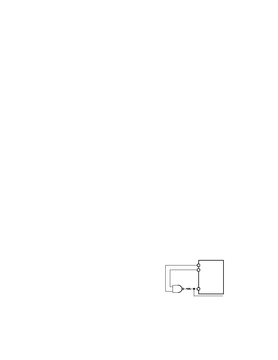
pins are those desired is to construct a circuit like the one shown
in Figure 12. This circuit forces the value located on the Mode
A pin to logic high; regardless if it latched via the
RESET or
ERESET pin.
PROGRAMMABLE I/O
MODE A/PFO
RESET
ERESET
1k
ADSP-2189M
Figure 12. Mode A Pin/EZ-ICE Circuit
See the ADSP-2100 Family EZ-Tools data sheet for complete
information on ICE products.
相关PDF资料 |
PDF描述 |
|---|---|
| VI-B1N-CX-B1 | CONVERTER MOD DC/DC 18.5V 75W |
| VE-21N-CY-F2 | CONVERTER MOD DC/DC 18.5V 50W |
| ADSP-21369KSWZ-5A | IC DSP 32BIT 366MHZ 208LQFP |
| TAP106M035BRW | CAP TANT 10UF 35V 20% RADIAL |
| XC2C384-10FGG324C | IC CR-II CPLD 384MCELL 324-FBGA |
相关代理商/技术参数 |
参数描述 |
|---|---|
| ADSP-2189MKSTZ-300 | 制造商:Analog Devices 功能描述:IC 16-BIT MICROCOMPUTER |
| ADSP-2189N | 制造商:AD 制造商全称:Analog Devices 功能描述:DSP Microcomputer |
| ADSP-2189NBCA-320 | 功能描述:IC DSP 16BIT 80MHZ 144CSPBGA RoHS:否 类别:集成电路 (IC) >> 嵌入式 - DSP(数字式信号处理器) 系列:ADSP-21xx 标准包装:2 系列:StarCore 类型:SC140 内核 接口:DSI,以太网,RS-232 时钟速率:400MHz 非易失内存:外部 芯片上RAM:1.436MB 电压 - 输入/输出:3.30V 电压 - 核心:1.20V 工作温度:-40°C ~ 105°C 安装类型:表面贴装 封装/外壳:431-BFBGA,FCBGA 供应商设备封装:431-FCPBGA(20x20) 包装:托盘 |
| ADSP-2189NBCAZ-320 | 功能描述:IC DSP 16BIT 80MHZ 144CSPBGA RoHS:是 类别:集成电路 (IC) >> 嵌入式 - DSP(数字式信号处理器) 系列:ADSP-21xx 标准包装:2 系列:StarCore 类型:SC140 内核 接口:DSI,以太网,RS-232 时钟速率:400MHz 非易失内存:外部 芯片上RAM:1.436MB 电压 - 输入/输出:3.30V 电压 - 核心:1.20V 工作温度:-40°C ~ 105°C 安装类型:表面贴装 封装/外壳:431-BFBGA,FCBGA 供应商设备封装:431-FCPBGA(20x20) 包装:托盘 |
| ADSP-2189NBCAZ-3202 | 制造商:AD 制造商全称:Analog Devices 功能描述:DSP Microcomputer |
发布紧急采购,3分钟左右您将得到回复。