- 您现在的位置:买卖IC网 > PDF目录19389 > ADSP-BF532SBBZ400 (Analog Devices Inc)IC DSP CTLR 16BIT 400MHZ 169-BGA PDF资料下载
参数资料
| 型号: | ADSP-BF532SBBZ400 |
| 厂商: | Analog Devices Inc |
| 文件页数: | 45/64页 |
| 文件大小: | 0K |
| 描述: | IC DSP CTLR 16BIT 400MHZ 169-BGA |
| 产品培训模块: | Blackfin® Processor Core Architecture Overview Blackfin® Device Drivers Blackfin® Optimizations for Performance and Power Consumption Blackfin® System Services |
| 标准包装: | 1 |
| 系列: | Blackfin® |
| 类型: | 定点 |
| 接口: | SPI,SSP,UART |
| 时钟速率: | 400MHz |
| 非易失内存: | ROM(1 kB) |
| 芯片上RAM: | 84kB |
| 电压 - 输入/输出: | 3.30V |
| 电压 - 核心: | 1.20V |
| 工作温度: | -40°C ~ 85°C |
| 安装类型: | 表面贴装 |
| 封装/外壳: | 169-BBGA |
| 供应商设备封装: | 169-PBGA(19x19) |
| 包装: | 托盘 |
| 配用: | ADZS-BF533-EZLITE-ND - KIT W/BOARD EVAL FOR ADSP-BF533 |
第1页第2页第3页第4页第5页第6页第7页第8页第9页第10页第11页第12页第13页第14页第15页第16页第17页第18页第19页第20页第21页第22页第23页第24页第25页第26页第27页第28页第29页第30页第31页第32页第33页第34页第35页第36页第37页第38页第39页第40页第41页第42页第43页第44页当前第45页第46页第47页第48页第49页第50页第51页第52页第53页第54页第55页第56页第57页第58页第59页第60页第61页第62页第63页第64页
�� �
�
�ADSP-BF531� /� ADSP-BF532� /� ADSP-BF533�
�TEST� CONDITIONS�
�All� timing� parameters� appearing� in� this� data� sheet� were� mea-�
��shows� the� measurement� point� for� ac� measurements� (except� out-�
�put� enable/disable).� The� measurement� point� V� MEAS� is� 0.95� V� for�
�V� DDEXT� (nominal)� =� 1.8� V� or� 1.5� V� for� V� DDEXT� (nominal)� =� 2.5� V/�
�The� time� t� DECAY� is� calculated� with� test� loads� C� L� and� I� L� ,� and� with�
�?� V� equal� to� 0.1� V� for� V� DDEXT� (nominal)� =� 1.8� V� or� 0.5� V� for�
�V� DDEXT� (nominal)� =� 2.5� V/3.3� V.�
�The� time� t� DIS_MEASURED� is� the� interval� from� when� the� reference�
�signal� switches,� to� when� the� output� voltage� decays� ?� V� from� the�
�measured� output� high� or� output� low� voltage.�
�3.3� V.�
�REFERENCE�
�SIGNAL�
�INPUT�
�OR�
�OUTPUT�
�V� MEAS�
�V� MEAS�
�t� DIS_MEASURED�
�t� ENA_MEASURED�
�t� DIS�
�t� ENA�
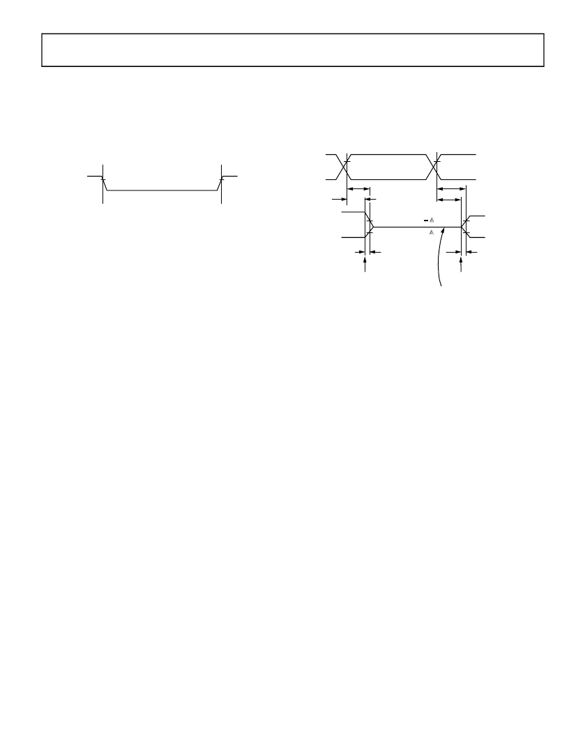
�Figure� 45.� Voltage� Reference� Levels� for� AC�
�Measurements� (Except� Output� Enable/Disable)�
�Output� Enable� Time� Measurement�
�V� OH�
�(MEASURED)�
�V� OL�
�(MEASURED)�
�V� OH� (MEASURED)�
�V� OL� (MEASURED)� +�
�t� DECAY�
�V�
�V�
�V� OH� (MEASURED)�
�V� TRIP� (HIGH)�
�V� TRIP� (LOW)�
�V� OL� (MEASURED)�
�t� TRIP�
�Output� pins� are� considered� to� be� enabled� when� they� have� made�
�a� transition� from� a� high� impedance� state� to� the� point� when� they�
�start� driving.�
�OUTPUT� STOPS� DRIVING�
�OUTPUT� STARTS� DRIVING�
�The� output� enable� time� t� ENA� is� the� interval� from� the� point� when�
�a� reference� signal� reaches� a� high� or� low� voltage� level� to� the� point�
�when� the� output� starts� driving� as� shown� on� the� right� side� of�
��The� time� t� ENA_MEASURED� is� the� interval,� from� when� the� reference�
�signal� switches,� to� when� the� output� voltage� reaches� V� TRIP� (high)�
�or� V� TRIP� (low).�
�For� V� DDEXT� (nominal)� =� 1.8� V—V� TRIP� (high)� is� 1.3� V� and� V� TRIP�
�(low)� is� 0.7� V.�
�For� V� DDEXT� (nominal)� =� 2.5� V/3.3� V—V� TRIP� (high)� is� 2.0� V� and�
�V� TRIP� (low)� is� 1.0� V.�
�Time� t� TRIP� is� the� interval� from� when� the� output� starts� driving� to�
�when� the� output� reaches� the� V� TRIP� (high)� or� V� TRIP� (low)� trip�
�voltage.�
�Time� t� ENA� is� calculated� as� shown� in� the� equation:�
�t� ENA� =� t� ENA_MEASURED� –� t� TRIP�
�If� multiple� pins� (such� as� the� data� bus)� are� enabled,� the� measure-�
�ment� value� is� that� of� the� first� pin� to� start� driving.�
�Output� Disable� Time� Measurement�
�Output� pins� are� considered� to� be� disabled� when� they� stop� driv-�
�ing,� go� into� a� high� impedance� state,� and� start� to� decay� from� their�
�output� high� or� low� voltage.� The� output� disable� time� t� DIS� is� the�
�difference� between� t� DIS_MEASURED� and� t� DECAY� as� shown� on� the� left�
��t� DIS� =� t� DIS_MEASURED� –� t� DECAY�
�The� time� for� the� voltage� on� the� bus� to� decay� by� ?� V� is� dependent�
�on� the� capacitive� load� C� L� and� the� load� current� I� I� .� This� decay� time�
�can� be� approximated� by� the� equation:�
�t� DECAY� =� ?� C� L� ?� V� ?� ?� I� L�
�HIGH� IMPEDANCE� STATE�
�Figure� 46.� Output� Enable/Disable�
�Example� System� Hold� Time� Calculation�
�To� determine� the� data� output� hold� time� in� a� particular� system,�
�first� calculate� t� DECAY� using� the� equation� given� above.� Choose� ?� V�
�to� be� the� difference� between� the� processor’s� output� voltage� and�
�the� input� threshold� for� the� device� requiring� the� hold� time.� C� L� is�
�the� total� bus� capacitance� (per� data� line),� and� I� L� is� the� total� leak-�
�age� or� three-state� current� (per� data� line).� The� hold� time� is� t� DECAY�
�plus� the� various� output� disable� times� as� specified� in� the� Timing�
��write� cycle� as� shown� in� SDRAM� Interface� Timing� on� Page� 30� ).�
�Rev.� I�
�|�
�Page� 45� of� 64� |�
�August� 2013�
�相关PDF资料 |
PDF描述 |
|---|---|
| ADSP-BF542BBCZ-4A | IC DSP 16BIT 400MHZ 400CSBGA |
| HBM12DRYN | CONN EDGECARD 24POS DIP .156 SLD |
| RMA30DTBD-S273 | CONN EDGECARD 60POS R/A .125 SLD |
| MAX6505UTP015+T | IC TEMP SWITCH DL TRIP SOT23-6 |
| RSA30DTAD-S273 | CONN EDGECARD 60POS R/A .125 SLD |
相关代理商/技术参数 |
参数描述 |
|---|---|
| ADSP-BF532SBST-300 | 制造商:Analog Devices 功能描述: |
| ADSPBF532SBST400 | 制造商:Analog Devices 功能描述: |
| ADSP-BF532SBST400 | 制造商:Analog Devices 功能描述:DSP Fixed-Point 16-Bit 400MHz 400MIPS 176-Pin LQFP 制造商:Analog Devices 功能描述:IC MICROCOMPUTER 16-BIT |
| ADSP-BF532SBST-DAB | 制造商:Analog Devices 功能描述: |
| ADSP-BF532SBSTZ400 | 功能描述:IC DSP CTLR 16BIT 400MHZ 176LQFP RoHS:是 类别:集成电路 (IC) >> 嵌入式 - DSP(数字式信号处理器) 系列:Blackfin® 标准包装:40 系列:TMS320DM64x, DaVinci™ 类型:定点 接口:I²C,McASP,McBSP 时钟速率:400MHz 非易失内存:外部 芯片上RAM:160kB 电压 - 输入/输出:3.30V 电压 - 核心:1.20V 工作温度:0°C ~ 90°C 安装类型:表面贴装 封装/外壳:548-BBGA,FCBGA 供应商设备封装:548-FCBGA(27x27) 包装:托盘 配用:TMDSDMK642-0E-ND - DEVELPER KIT W/NTSC CAMERA296-23038-ND - DSP STARTER KIT FOR TMS320C6416296-23059-ND - FLASHBURN PORTING KIT296-23058-ND - EVAL MODULE FOR DM642TMDSDMK642-ND - DEVELOPER KIT W/NTSC CAMERA |
发布紧急采购,3分钟左右您将得到回复。