- 您现在的位置:买卖IC网 > PDF目录19311 > ADSP-BF561SKB500 (Analog Devices Inc)IC DSP CTRLR 32BIT 500MHZ 297BGA PDF资料下载
参数资料
| 型号: | ADSP-BF561SKB500 |
| 厂商: | Analog Devices Inc |
| 文件页数: | 12/64页 |
| 文件大小: | 0K |
| 描述: | IC DSP CTRLR 32BIT 500MHZ 297BGA |
| 产品培训模块: | Blackfin® Processor Core Architecture Overview Blackfin® Device Drivers Blackfin® Optimizations for Performance and Power Consumption Blackfin® System Services |
| 产品变化通告: | Product Discontinuance 27/Oct/2011 |
| 标准包装: | 1 |
| 系列: | Blackfin® |
| 类型: | 定点 |
| 接口: | SPI,SSP,UART |
| 时钟速率: | 500MHz |
| 非易失内存: | 外部 |
| 芯片上RAM: | 328kB |
| 电压 - 输入/输出: | 2.50V,3.30V |
| 电压 - 核心: | 1.25V |
| 工作温度: | 0°C ~ 70°C |
| 安装类型: | 表面贴装 |
| 封装/外壳: | 297-BGA |
| 供应商设备封装: | 297-PBGA(27x27) |
| 包装: | 托盘 |
| 配用: | ADZS-BFAUDIO-EZEXT-ND - BOARD EVAL AUDIO BLACKFIN ADZS-BF561-EZLITE-ND - BOARD EVAL ADSP-BF561 ADZS-BF561-MMSKIT-ND - KIT STARTER MULTIMEDIA BF561 ADZS-BFAV-EZEXT-ND - BOARD DAUGHT ADSP-BF533,37,61KIT |
第1页第2页第3页第4页第5页第6页第7页第8页第9页第10页第11页当前第12页第13页第14页第15页第16页第17页第18页第19页第20页第21页第22页第23页第24页第25页第26页第27页第28页第29页第30页第31页第32页第33页第34页第35页第36页第37页第38页第39页第40页第41页第42页第43页第44页第45页第46页第47页第48页第49页第50页第51页第52页第53页第54页第55页第56页第57页第58页第59页第60页第61页第62页第63页第64页
�� �
�
�ADSP-BF561 �
�regulator� for� the� processor� can� be� shut� off� by� writing� b#00� to� the�
�FREQ� bits� of� the� VR_CTL� register.� This� disables� both� CCLK�
�and� SCLK.� Furthermore,� it� sets� the� internal� power� supply� volt-�
�age� (V� DDINT� )� to� 0� V� to� provide� the� lowest� static� power� dissipation.�
�Any� critical� information� stored� internally� (memory� contents,�
�register� contents,� etc.)� must� be� written� to� a� nonvolatile� storage�
�device� prior� to� removing� power� if� the� processor� state� is� to� be�
�preserved.� Since� V� DDEXT� is� still� supplied� in� this� mode,� all� of� the�
�external� pins� three-state,� unless� otherwise� specified.� This� allows�
�other� devices� that� may� be� connected� to� the� processor� to� have�
�power� still� applied� without� drawing� unwanted� current.� The�
�interna� l� supply� regulator� can� be� woken� up� by� asserting� the�
�RESET� pin.�
�Power� Savings�
�As� shown� in� Table� 4� ,� the� ADSP-BF561� supports� two� different�
�power� domains.� The� use� of� multiple� power� domains� maximizes�
�flexibility,� while� maintaining� compliance� with� industry� stan-�
�dards� and� conventions.� By� isolating� the� internal� logic� of� the�
�ADSP-BF561� into� its� own� power� domain,� separate� from� the� I/O,�
�the� processor� can� take� advantage� of� Dynamic� Power� Manage-�
�ment,� without� affecting� the� I/O� devices.� There� are� no�
�sequencing� requirements� for� the� various� power� domains.�
�Table� 4.� ADSP-BF561� Power� Domains�
�t� NOM� is� the� duration� running� at� f� CCLKNOM�
�t� RED� is� the� duration� running� at� f� CCLKRED�
�The� percent� power� savings� is� calculated� as:�
�%� power� savings� =� (� 1� –� power� savings� factor� )� ×� 100%�
�VOLTAGE� REGULATION�
�The� ADSP-BF561� processor� provides� an� on-chip� voltage� regula-�
�tor� that� can� generate� appropriate� V� DDINT� voltage� levels� from� the�
�V� DDEXT� supply.� See� Operating� Conditions� on� Page� 20� for� regula-�
�tor� tolerances� and� acceptable� V� DDEXT� ranges� for� specific� models.�
��complete� the� power� management� system.� The� regulator� con-�
�trols� the� internal� logic� voltage� levels� and� is� programmable� with�
�the� voltage� regulator� control� register� (VR_CTL)� in� increments�
�of� 50� mV.� To� reduce� standby� power� consumption,� the� internal�
�voltage� regulator� can� be� programmed� to� remove� power� to� the�
�processor� core� while� keeping� I/O� power� (V� DDEXT� )� supplied.� While�
�in� the� hibernate� state,� V� DDEXT� can� still� be� applied,� thus� eliminating�
�the� need� for� external� buffers.� The� voltage� regulator� can� be� acti-�
�vated� from� this� power-down� state� by� asserting� RESET,� which�
�will� then� initiate� a� boot� sequence.� The� regulator� can� also� be� dis-�
�abled� and� bypassed� at� the� user’s� discretion.�
�The� internal� voltage� regulation� feature� is� not� available� on� any� of�
�Power� Domain�
�All� internal� logic�
�I/O�
�V� DD� Range�
�V� DDINT�
�V� DDEXT�
�the� 600� MHz� speed� grade� models� or� automotive� grade� models.�
�External� voltage� regulation� is� required� to� ensure� correct� opera-�
�tion� of� these� parts� at� 600� MHz.�
�The� power� dissipated� by� a� processor� is� largely� a� function� of� the�
�clock� frequency� of� the� processor� and� the� square� of� the� operating�
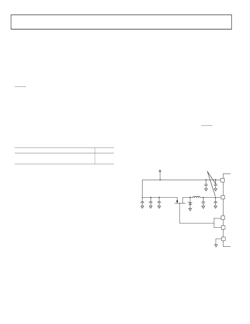
�V� DDEXT�
�(LOW-INDUCTANCE) �
�SET� OF� DECOUPLING �
�CAPACITORS�
�voltage.� For� example,� reducing� the� clock� frequency� by� 25%�
�results� in� a� 25%� reduction� in� dynamic� power� dissipation,� while�
�reducing� the� voltage� by� 25%� reduces� dynamic� power� dissipation�
�100μF�
�+�
�V� DDEXT�
�by� more� than� 40%.� Further,� these� power� savings� are� additive,� in�
�100nF�
�10μH�
�that� if� the� clock� frequency� and� supply� voltage� are� both� reduced,�
�the� power� savings� can� be� dramatic.�
�100μF�
�+�
�+�
�V� DDINT�
�The� dynamic� power� management� feature� of� the� ADSP-BF561�
�allows� both� the� processor’s� input� voltage� (V� DDINT� )� and� clock� fre-�
�quency� (f� CCLK� )� to� be� dynamically� controlled.�
�10μF�
�LOW� ESR�
�FDS9431A�
�ZHCS1000�
�100μF�
�VR� OUT�
�The� savings� in� power� dissipation� can� be� modeled� using� the�
�=� ---------------------� � ?� ?� --------------------------� ?� ?� � ??� -----------� ??�
�power� savings� factor� and� %� power� savings� calculations.�
�The� power� savings� factor� is� calculated� as:�
�power� savings� factor�
�f� CCLKRED� V� DDINTRED� 2� t� RED�
�f� CCLKNOM� V� DDINTNOM� t� NOM�
�where� the� variables� in� the� equations� are:�
�f� CCLKNOM� is� the� nominal� core� clock� frequency�
�f� CCLKRED� is� the� reduced� core� clock� frequency�
�V� DDINTNOM� is� the� nominal� internal� supply� voltage�
�V� DDINTRED� is� the� reduced� internal� supply� voltage�
�SHORT� AND� LOW-�
�INDUCTANCE� WIRE�
�NOTE:� DESIGNER� SHOULD� MINIMIZE�
�TRACE� LENGTH� TO� FDS9431A.�
�Figure� 4.� Voltage� Regulator� Circuit�
�Voltage� Regulator� Layout� Guidelines�
�Regulator� external� component� placement,� board� routing,� and�
�bypass� capacitors� all� have� a� significant� effect� on� noise� injected�
�into� the� other� analog� circuits� on-chip.� The� VROUT1–0� traces�
�and� voltage� regulator� external� components� should� be� consid-�
�ered� as� noise� sources� when� doing� board� layout� and� should� not�
�VR� OUT�
�GND�
�be� routed� or� placed� near� sensitive� circuits� or� components� on� the�
�Rev.� E� |�
�Page� 12� of� 64� |�
�September� 2009�
�相关PDF资料 |
PDF描述 |
|---|---|
| GEM10DTKN | CONN EDGECARD 20POS DIP .156 SLD |
| EEM11DRTH | CONN EDGECARD 22POS DIP .156 SLD |
| RSM36DRYI | CONN EDGECARD 72POS DIP .156 SLD |
| GEM10DTKH | CONN EDGECARD 20POS DIP .156 SLD |
| EBM06DRSS | CONN EDGECARD 12POS DIP .156 SLD |
相关代理商/技术参数 |
参数描述 |
|---|---|
| ADSP-BF561SKB600 | 功能描述:IC DSP CTRLR 32BIT 600MHZ 297BGA RoHS:否 类别:集成电路 (IC) >> 嵌入式 - DSP(数字式信号处理器) 系列:Blackfin® 标准包装:2 系列:StarCore 类型:SC140 内核 接口:DSI,以太网,RS-232 时钟速率:400MHz 非易失内存:外部 芯片上RAM:1.436MB 电压 - 输入/输出:3.30V 电压 - 核心:1.20V 工作温度:-40°C ~ 105°C 安装类型:表面贴装 封装/外壳:431-BFBGA,FCBGA 供应商设备封装:431-FCPBGA(20x20) 包装:托盘 |
| ADSP-BF561SKB750 | 制造商:Analog Devices 功能描述: |
| ADSP-BF561SKBCZ500 | 功能描述:BLACK FIN, EMBEDDED,SYMMETRIC RoHS:是 类别:集成电路 (IC) >> 嵌入式 - DSP(数字式信号处理器) 系列:Blackfin® 标准包装:2 系列:StarCore 类型:SC140 内核 接口:DSI,以太网,RS-232 时钟速率:400MHz 非易失内存:外部 芯片上RAM:1.436MB 电压 - 输入/输出:3.30V 电压 - 核心:1.20V 工作温度:-40°C ~ 105°C 安装类型:表面贴装 封装/外壳:431-BFBGA,FCBGA 供应商设备封装:431-FCPBGA(20x20) 包装:托盘 |
| ADSP-BF561SKBCZ-5A | 功能描述:IC DSP CTLR 32BIT BKFN 256CSPBGA RoHS:是 类别:集成电路 (IC) >> 嵌入式 - DSP(数字式信号处理器) 系列:Blackfin® 标准包装:40 系列:TMS320DM64x, DaVinci™ 类型:定点 接口:I²C,McASP,McBSP 时钟速率:400MHz 非易失内存:外部 芯片上RAM:160kB 电压 - 输入/输出:3.30V 电压 - 核心:1.20V 工作温度:0°C ~ 90°C 安装类型:表面贴装 封装/外壳:548-BBGA,FCBGA 供应商设备封装:548-FCBGA(27x27) 包装:托盘 配用:TMDSDMK642-0E-ND - DEVELPER KIT W/NTSC CAMERA296-23038-ND - DSP STARTER KIT FOR TMS320C6416296-23059-ND - FLASHBURN PORTING KIT296-23058-ND - EVAL MODULE FOR DM642TMDSDMK642-ND - DEVELOPER KIT W/NTSC CAMERA |
| ADSP-BF561SKBCZ-5V | 功能描述:IC DSP 32BIT 500MHZ 256CSPBGA RoHS:是 类别:集成电路 (IC) >> 嵌入式 - DSP(数字式信号处理器) 系列:Blackfin® 标准包装:2 系列:StarCore 类型:SC140 内核 接口:DSI,以太网,RS-232 时钟速率:400MHz 非易失内存:外部 芯片上RAM:1.436MB 电压 - 输入/输出:3.30V 电压 - 核心:1.20V 工作温度:-40°C ~ 105°C 安装类型:表面贴装 封装/外壳:431-BFBGA,FCBGA 供应商设备封装:431-FCPBGA(20x20) 包装:托盘 |
发布紧急采购,3分钟左右您将得到回复。