参数资料
| 型号: | ADUC816BCP |
| 厂商: | Analog Devices Inc |
| 文件页数: | 54/68页 |
| 文件大小: | 0K |
| 描述: | IC MCU 8K FLASH ADC/DAC 56LFCSP |
| 标准包装: | 1 |
| 系列: | MicroConverter® ADuC8xx |
| 核心处理器: | 8052 |
| 芯体尺寸: | 8-位 |
| 速度: | 12.58MHz |
| 连通性: | I²C,SPI,UART/USART |
| 外围设备: | PSM,温度传感器,WDT |
| 输入/输出数: | 34 |
| 程序存储器容量: | 8KB(8K x 8) |
| 程序存储器类型: | 闪存 |
| EEPROM 大小: | 640 x 8 |
| RAM 容量: | 256 x 8 |
| 电压 - 电源 (Vcc/Vdd): | 2.7 V ~ 5.5 V |
| 数据转换器: | A/D 7x16b; D/A 1x12b |
| 振荡器型: | 内部 |
| 工作温度: | -40°C ~ 85°C |
| 封装/外壳: | 56-VFQFN 裸露焊盘,CSP |
| 包装: | 托盘 |
| 产品目录页面: | 738 (CN2011-ZH PDF) |
第1页第2页第3页第4页第5页第6页第7页第8页第9页第10页第11页第12页第13页第14页第15页第16页第17页第18页第19页第20页第21页第22页第23页第24页第25页第26页第27页第28页第29页第30页第31页第32页第33页第34页第35页第36页第37页第38页第39页第40页第41页第42页第43页第44页第45页第46页第47页第48页第49页第50页第51页第52页第53页当前第54页第55页第56页第57页第58页第59页第60页第61页第62页第63页第64页第65页第66页第67页第68页
REV. 0
ADuC816
–58–
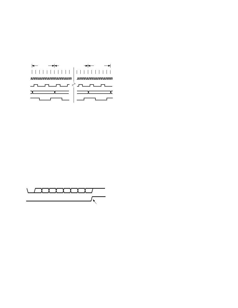
Mode 0: 8-Bit Shift Register Mode
Mode 0 is selected by clearing both the SM0 and SM1 bits in
the SFR SCON. Serial data enters and exits through RXD. TXD
outputs the shift clock. Eight data bits are transmitted or received.
Transmission is initiated by any instruction that writes to SBUF.
The data is shifted out of the RXD line. The eight bits are trans-
mitted with the least-significant bit (LSB) first, as shown in
Figure 39.
CORE
CLK
ALE
RXD
(DATA OUT)
TXD
(SHIFT CLOCK)
DATA BIT 0
DATA BIT 1
DATA BIT 6
DATA BIT 7
S6
S5
S4
S3
S2
S1
S6
S5
S4
S3
S2
S1
S6
S5
S4
S3
S2
S1
MACHINE
CYCLE 8
MACHINE
CYCLE 7
MACHINE
CYCLE 2
MACHINE
CYCLE 1
Figure 39. UART Serial Port Transmission, Mode 0
Reception is initiated when the receive enable bit (REN) is 1 and
the receive interrupt bit (RI) is 0. When RI is cleared the data is
clocked into the RXD line and the clock pulses are output from
the TXD line.
Mode 1: 8-Bit UART, Variable Baud Rate
Mode 1 is selected by clearing SM0 and setting SM1. Each data
byte (LSB first) is preceded by a start bit(0) and followed by a stop
bit(1). Therefore 10 bits are transmitted on TXD or received on
RXD. The baud rate is set by the Timer 1 or Timer 2 overflow
rate, or a combination of the two (one for transmission and the
other for reception).
Transmission is initiated by writing to SBUF. The “write to
SBUF” signal also loads a 1 (stop bit) into the ninth bit position
of the transmit shift register. The data is output bit by bit until
the stop bit appears on TXD and the transmit interrupt flag (TI)
is automatically set as shown in Figure 40.
TXD
TI
(SCON.1)
START
BIT
D0
D1
D2
D3
D4
D5
D6
D7
STOP BIT
SET INTERRUPT
i.e., READY FOR MORE DATA
Figure 40. UART Serial Port Transmission, Mode 0
Reception is initiated when a 1-to-0 transition is detected on
RXD. Assuming a valid start bit was detected, character reception
continues. The start bit is skipped and the eight data bits are
clocked into the serial port shift register. When all eight bits have
been clocked in, the following events occur:
The eight bits in the receive shift register are latched into SBUF
The ninth bit (Stop bit) is clocked into RB8 in SCON
The Receiver interrupt flag (RI) is set
if, and only if, the following conditions are met at the time the
final shift pulse is generated:
RI = 0, and
Either SM2 = 0, or SM2 = 1 and the received stop bit = 1.
If either of these conditions is not met, the received frame is
irretrievably lost, and RI is not set.
Mode 2: 9-Bit UART with Fixed Baud Rate
Mode 2 is selected by setting SM0 and clearing SM1. In this
mode the UART operates in 9-bit mode with a fixed baud rate.
The baud rate is fixed at Core_Clk/64 by default, although by
setting the SMOD bit in PCON, the frequency can be doubled to
Core_Clk/32. Eleven bits are transmitted or received, a start bit(0),
eight data bits, a programmable ninth bit and a stop bit(1). The
ninth bit is most often used as a parity bit, although it can be used
for anything, including a ninth data bit if required.
To transmit, the eight data bits must be written into SBUF. The
ninth bit must be written to TB8 in SCON. When transmission is
initiated the eight data bits (from SBUF) are loaded onto the
transmit shift register (LSB first). The contents of TB8 are loaded
into the ninth bit position of the transmit shift register. The trans-
mission will start at the next valid baud rate clock. The TI flag
is set as soon as the stop bit appears on TXD.
Reception for Mode 2 is similar to that of Mode 1. The eight
data bytes are input at RXD (LSB first) and loaded onto the
receive shift register. When all eight bits have been clocked in,
the following events occur:
The eight bits in the receive shift register are latched into SBUF
The ninth data bit is latched into RB8 in SCON
The Receiver interrupt flag (RI) is set
if, and only if, the following conditions are met at the time the
final shift pulse is generated:
RI = 0, and
Either SM2 = 0, or SM2 = 1 and the received stop bit = 1.
If either of these conditions is not met, the received frame is
irretrievably lost, and RI is not set.
Mode 3: 9-Bit UART with Variable Baud Rate
Mode 3 is selected by setting both SM0 and SM1. In this mode
the 8051 UART serial port operates in 9-bit mode with a variable
baud rate determined by either Timer 1 or Timer 2. The opera-
tion of the 9-bit UART is the same as for Mode 2 but the baud
rate can be varied as for Mode 1.
In all four modes, transmission is initiated by any instruction that
uses SBUF as a destination register. Reception is initiated in Mode 0
by the condition RI = 0 and REN = 1. Reception is initiated in
the other modes by the incoming start bit if REN = 1.
UART Serial Port Baud Rate Generation
Mode 0 Baud Rate Generation
The baud rate in Mode 0 is fixed:
Mode 0 Baud Rate = (Core Clock Frequency
1/12)
NOTE
1In these descriptions Core Clock Frequency refers to the core clock frequency
selected via the CD0–2 bits in the PLLCON SFR.
Mode 2 Baud Rate Generation
The baud rate in Mode 2 depends on the value of the SMOD bit
in the PCON SFR. If SMOD = 0, the baud rate is 1/64 of the core
clock. If SMOD = 1, the baud rate is 1/32 of the core clock:
Mode 2 Baud Rate = (2
SMOD/64)
× (Core Clock Frequency)
Modes 1 and 3 Baud Rate Generation
The baud rates in Modes 1 and 3 are determined by the overflow
rate in Timer 1 or Timer 2, or both (one for transmit and the
other for receive).
REV. A
相关PDF资料 |
PDF描述 |
|---|---|
| ADUC824BSZ-REEL | IC MCU 8K FLASH ADC/DAC 52MQFP |
| ADUC831BCPZ | IC MCU 62K FLASH ADC/DAC 56LFCSP |
| ADUC832BSZ-REEL | IC MCU 62K FLASH ADC/DAC 52MQFP |
| ADUC834BCPZ-REEL | IC MCU 62K FLASH ADC/DAC 56LFCSP |
| ADUC836BCPZ | IC MCU 62K FLASH ADC/DAC 56LFCSP |
相关代理商/技术参数 |
参数描述 |
|---|---|
| ADUC816BCP-REEL | 制造商:Analog Devices 功能描述:MCU 8-Bit ADuC8xx 8052 CISC 8KB Flash 3.3V/5V 56-Pin LFCSP EP T/R 制造商:Analog Devices 功能描述:MCU 8BIT CISC 8KB FLASH 3.3V/5V 56LFCSP EP - Tape and Reel |
| ADUC816BCPZ | 功能描述:IC MCU FLASH 16BIT ADC 56LFCSP RoHS:是 类别:集成电路 (IC) >> 嵌入式 - 微控制器, 系列:MicroConverter® ADuC8xx 标准包装:38 系列:Encore!® XP® 核心处理器:eZ8 芯体尺寸:8-位 速度:5MHz 连通性:IrDA,UART/USART 外围设备:欠压检测/复位,LED,POR,PWM,WDT 输入/输出数:16 程序存储器容量:4KB(4K x 8) 程序存储器类型:闪存 EEPROM 大小:- RAM 容量:1K x 8 电压 - 电源 (Vcc/Vdd):2.7 V ~ 3.6 V 数据转换器:- 振荡器型:内部 工作温度:-40°C ~ 105°C 封装/外壳:20-SOIC(0.295",7.50mm 宽) 包装:管件 其它名称:269-4116Z8F0413SH005EG-ND |
| ADUC816BCPZ-REEL | 功能描述:8052 MicroConverter? ADuC8xx Microcontroller IC 8-Bit 12.58MHz 8KB (8K x 8) FLASH 56-LFCSP (8x8) 制造商:analog devices inc. 系列:MicroConverter? ADuC8xx 包装:带卷(TR) 零件状态:上次购买时间 核心处理器:8052 核心尺寸:8-位 速度:12.58MHz 连接性:I2C,SPI,UART/USART 外设:PSM,温度传感器,WDT I/O 数:34 程序存储容量:8KB(8K x 8) 程序存储器类型:闪存 EEPROM 容量:640 x 8 RAM 容量:256 x 8 电压 - 电源(Vcc/Vdd):2.7 V ~ 5.5 V 数据转换器:A/D 7x16b;D/A 1x12b 振荡器类型:内部 工作温度:-40°C ~ 85°C(TA) 封装/外壳:56-WFQFN 裸焊盘,CSP 供应商器件封装:56-LFCSP (8x8) 标准包装:1 |
| ADUC816BS | 制造商:Analog Devices 功能描述:MCU 8-Bit ADuC8xx 8052 CISC 8KB Flash 3.3V/5V 52-Pin MQFP 制造商:Rochester Electronics LLC 功能描述:8BIT CISC 8KB FLASH 12.58MHZ 3.3/5V 52MQFP - Bulk 制造商:Analog Devices 功能描述:8BIT MCU +16BIT ADC MQFP52 816 |
| ADUC816BS-REEL | 制造商:Analog Devices 功能描述:MCU 8-Bit ADuC8xx 8052 CISC 8KB Flash 3.3V/5V 52-Pin MQFP T/R |
发布紧急采购,3分钟左右您将得到回复。