- 您现在的位置:买卖IC网 > PDF目录11203 > ADUC848BSZ8-3 (Analog Devices Inc)IC MCU FLASH W/16BIT ADC 52MQFP PDF资料下载
参数资料
| 型号: | ADUC848BSZ8-3 |
| 厂商: | Analog Devices Inc |
| 文件页数: | 26/108页 |
| 文件大小: | 0K |
| 描述: | IC MCU FLASH W/16BIT ADC 52MQFP |
| 标准包装: | 96 |
| 系列: | MicroConverter® ADuC8xx |
| 核心处理器: | 8052 |
| 芯体尺寸: | 8-位 |
| 速度: | 12.58MHz |
| 连通性: | I²C,SPI,UART/USART |
| 外围设备: | POR,PSM,PWM,温度传感器,WDT |
| 输入/输出数: | 34 |
| 程序存储器容量: | 8KB(8K x 8) |
| 程序存储器类型: | 闪存 |
| EEPROM 大小: | 4K x 8 |
| RAM 容量: | 2.25K x 8 |
| 电压 - 电源 (Vcc/Vdd): | 2.7 V ~ 3.6 V |
| 数据转换器: | A/D 10x16b; D/A 1x12b,2x16b |
| 振荡器型: | 内部 |
| 工作温度: | -40°C ~ 125°C |
| 封装/外壳: | 52-QFP |
| 包装: | 托盘 |
第1页第2页第3页第4页第5页第6页第7页第8页第9页第10页第11页第12页第13页第14页第15页第16页第17页第18页第19页第20页第21页第22页第23页第24页第25页当前第26页第27页第28页第29页第30页第31页第32页第33页第34页第35页第36页第37页第38页第39页第40页第41页第42页第43页第44页第45页第46页第47页第48页第49页第50页第51页第52页第53页第54页第55页第56页第57页第58页第59页第60页第61页第62页第63页第64页第65页第66页第67页第68页第69页第70页第71页第72页第73页第74页第75页第76页第77页第78页第79页第80页第81页第82页第83页第84页第85页第86页第87页第88页第89页第90页第91页第92页第93页第94页第95页第96页第97页第98页第99页第100页第101页第102页第103页第104页第105页第106页第107页第108页
ADuC845/ADuC847/ADuC848
Data Sheet
Rev. C | Page 24 of 108
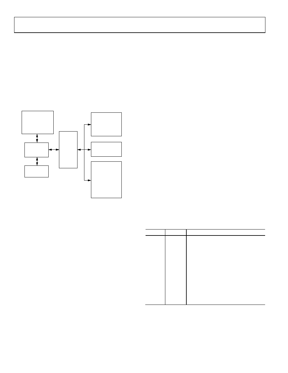
SPECIAL FUNCTION REGISTERS (SFRs)
The SFR space is mapped into the upper 128 bytes of internal
data memory space and accessed by direct addressing only. It
provides an interface between the CPU and all on-chip periph-
erals. A block diagram showing the programming model of the
ADuC845/ADuC847/ADuC848 via the SFR area is shown in
All registers except the program counter (PC) and the four
general-purpose register banks reside in the SFR area. The SFR
registers include control, configuration, and data registers that
provide an interface between the CPU and all on-chip peripherals.
128-BYTE
SPECIAL
FUNCTION
REGISTER
AREA
62-kBYTE
ELECTRICALLY
REPROGRAMMABLE
NONVOLATILE
FLASH/EE PROGRAM
MEMORY
8051-
COMPATIBLE
CORE
OTHER ON-CHIP
PERIPHERALS
TEMPERATURE
SENSOR
CURRENT SOURCES
12-BIT DAC
SERIAL I/O
WDT
PSM
TIC
PWM
S-D ADC
4-kBYTE
ELECTRICALLY
REPROGRAMMABLE
NONVOLATILE
FLASH/EE DATA
MEMORY
256 BYTES RAM
2kBYTES XRAM
04741-011
Figure 11. Programming Model
Accumulator SFR (ACC)
ACC is the accumulator register, which is used for math opera-
tions including addition, subtraction, integer multiplication and
division, and Boolean bit manipulations. The mnemonics for
accumulator-specific instructions usually refer to the
accumulator as A.
B SFR (B)
The B register is used with the accumulator for multiplication
and division operations. For other instructions, it can be treated
as a general-purpose scratch pad register.
Data Pointer (DPTR)
The data pointer is made up of three 8-bit registers: DPP (page
byte), DPH (high byte), and DPL (low byte). These provide
memory addresses for internal code and data memory access.
The DPTR can be manipulated as a 16-bit register (DPTR =
DPH, DPL), although INC DPTR instructions automatically
carry over to DPP, or as three independent 8-bit registers (DPP,
DPH, DPL).
The ADuC845/ADuC847/ADuC848 support dual data
pointers. See the Dual Data Pointers section.
Stack Pointer (SP and SPH)
The SP SFR is the stack pointer, which is used to hold an
internal RAM address called the top of the stack. The SP register
is incremented before data is stored during PUSH and CALL
executions. Although the stack can reside anywhere in on-chip
RAM, the SP register is initialized to 07H after a reset. This
causes the stack to begin at location 08H.
As mentioned earlier, the parts offer an extended 11-bit stack
pointer. The three extra bits needed to make up the 11-bit stack
pointer are the three LSBs of the SPH byte located at B7H. To
enable the SPH SFR, the EXSP (CFG84x.7) bit must be set;
otherwise, the SPH SFR can be neither written to nor read from.
Program Status Word (PSW)
The PSW SFR contains several bits that reflect the current
status of the CPU as listed in Table 5.
SFR Address:
D0H
Power-On Default:
00H
Bit Addressable:
Yes
Table 5. PSW SFR Bit Designations
Bit No.
Name
Description
7
CY
Carry Flag.
6
AC
Auxiliary Carry Flag.
5
F0
General-Purpose Flag.
4, 3
RS1, RS0
Register Bank Select Bits.
RS1
RS0
Selected Bank
0
1
0
2
1
3
2
OV
Overflow Flag.
1
F1
General-Purpose Flag.
0
P
Parity Bit.
相关PDF资料 |
PDF描述 |
|---|---|
| ADUC7020BCPZ62I-RL | IC MCU 12BIT 1MSPS I2C 40-LFCSP |
| ATXMEGA256A3B-MHR | IC MCU 8BIT 256KB FLASH 64VQFN |
| ATXMEGA256A3B-AUR | IC MCU 8BIT 256KB FLASH 64TQFP |
| VE-B33-IX-F2 | CONVERTER MOD DC/DC 24V 75W |
| VE-B33-IW-F4 | CONVERTER MOD DC/DC 24V 100W |
相关代理商/技术参数 |
参数描述 |
|---|---|
| ADUC848BSZ8-5 | 功能描述:IC MCU FLASH W/16BIT ADC 52MQFP RoHS:是 类别:集成电路 (IC) >> 嵌入式 - 微控制器, 系列:MicroConverter® ADuC8xx 标准包装:250 系列:LPC11Uxx 核心处理器:ARM? Cortex?-M0 芯体尺寸:32-位 速度:50MHz 连通性:I²C,Microwire,SPI,SSI,SSP,UART/USART,USB 外围设备:欠压检测/复位,POR,WDT 输入/输出数:40 程序存储器容量:96KB(96K x 8) 程序存储器类型:闪存 EEPROM 大小:4K x 8 RAM 容量:10K x 8 电压 - 电源 (Vcc/Vdd):1.8 V ~ 3.6 V 数据转换器:A/D 8x10b 振荡器型:内部 工作温度:-40°C ~ 85°C 封装/外壳:48-LQFP 包装:托盘 其它名称:568-9587 |
| AD-UCFS-JRN-SPRD | 功能描述:PRD LIC UCFS JOURNAL CCES 1 PRD RoHS:否 类别:编程器,开发系统 >> 软件 系列:* 标准包装:1 系列:ISE® 设计套件 类型:订阅 适用于相关产品:Xilinx FPGAs 其它名称:Q4986209T1081384 |
| AD-UCFS-MJRN-SP | 功能描述:PRD LIC UCFS JOURNAL MAIN 1 PRD RoHS:否 类别:编程器,开发系统 >> 软件 系列:* 标准包装:1 系列:ISE® 设计套件 类型:订阅 适用于相关产品:Xilinx FPGAs 其它名称:Q4986209T1081384 |
| AD-UCFS-MNT-SP | 功能描述:PRD LIC UCFS CORE MAIN 1 PRD RoHS:否 类别:编程器,开发系统 >> 软件 系列:* 标准包装:1 系列:ISE® 设计套件 类型:订阅 适用于相关产品:Xilinx FPGAs 其它名称:Q4986209T1081384 |
| AD-UCFS-SPRD | 功能描述:PRD LIC UCFS CORE CCES 1 PROD RoHS:否 类别:编程器,开发系统 >> 软件 系列:* 标准包装:1 系列:ISE® 设计套件 类型:订阅 适用于相关产品:Xilinx FPGAs 其它名称:Q4986209T1081384 |
发布紧急采购,3分钟左右您将得到回复。