- 您现在的位置:买卖IC网 > PDF目录11203 > ADUC848BSZ8-3 (Analog Devices Inc)IC MCU FLASH W/16BIT ADC 52MQFP PDF资料下载
参数资料
| 型号: | ADUC848BSZ8-3 |
| 厂商: | Analog Devices Inc |
| 文件页数: | 53/108页 |
| 文件大小: | 0K |
| 描述: | IC MCU FLASH W/16BIT ADC 52MQFP |
| 标准包装: | 96 |
| 系列: | MicroConverter® ADuC8xx |
| 核心处理器: | 8052 |
| 芯体尺寸: | 8-位 |
| 速度: | 12.58MHz |
| 连通性: | I²C,SPI,UART/USART |
| 外围设备: | POR,PSM,PWM,温度传感器,WDT |
| 输入/输出数: | 34 |
| 程序存储器容量: | 8KB(8K x 8) |
| 程序存储器类型: | 闪存 |
| EEPROM 大小: | 4K x 8 |
| RAM 容量: | 2.25K x 8 |
| 电压 - 电源 (Vcc/Vdd): | 2.7 V ~ 3.6 V |
| 数据转换器: | A/D 10x16b; D/A 1x12b,2x16b |
| 振荡器型: | 内部 |
| 工作温度: | -40°C ~ 125°C |
| 封装/外壳: | 52-QFP |
| 包装: | 托盘 |
第1页第2页第3页第4页第5页第6页第7页第8页第9页第10页第11页第12页第13页第14页第15页第16页第17页第18页第19页第20页第21页第22页第23页第24页第25页第26页第27页第28页第29页第30页第31页第32页第33页第34页第35页第36页第37页第38页第39页第40页第41页第42页第43页第44页第45页第46页第47页第48页第49页第50页第51页第52页当前第53页第54页第55页第56页第57页第58页第59页第60页第61页第62页第63页第64页第65页第66页第67页第68页第69页第70页第71页第72页第73页第74页第75页第76页第77页第78页第79页第80页第81页第82页第83页第84页第85页第86页第87页第88页第89页第90页第91页第92页第93页第94页第95页第96页第97页第98页第99页第100页第101页第102页第103页第104页第105页第106页第107页第108页
Data Sheet
ADuC845/ADuC847/ADuC848
Rev. C | Page 49 of 108
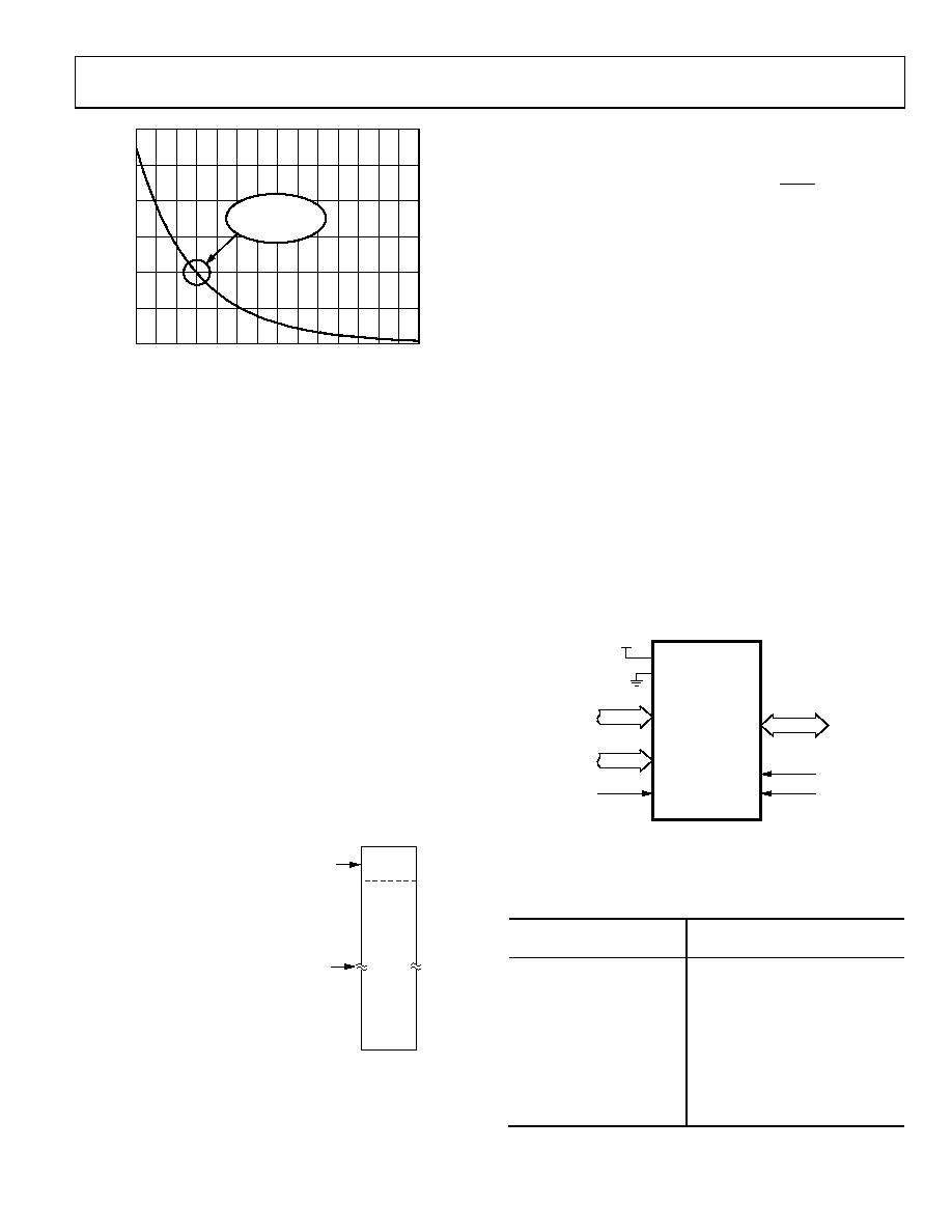
40
60
70
90
TJ JUNCTION TEMPERATURE (C)
RE
TE
NTION
(Years)
250
200
150
100
50
0
50
80
110
300
100
ADI SPECIFICATION
100 YEARS MIN.
AT TJ = 55C
04741-028
Figure 27. Flash/EE Memory Data Retention
FLASH/EE PROGRAM MEMORY
The ADuC845/ADuC847/ADuC848 contain a 64-kbyte array of
Flash/EE program memory. The lower 62 kbytes of this program
memory are available to the user for program storage or as
additional NV data memory.
The upper 2 kbytes of this Flash/EE program memory array
contain permanently embedded firmware, allowing in-circuit
serial download, serial debug, and nonintrusive single-pin
emulation. These 2 kbytes of embedded firmware also contain
a power-on configuration routine that downloads factory cali-
brated coefficients to the various calibrated peripherals such
as ADC, temperature sensor, current sources, band gap, and
references.
These 2 kbytes of embedded firmware are hidden from the user
code. Attempts to read this space read 0s; therefore, the embed-
ded firmware appears as NOP instructions to user code.
In normal operating mode (power-on default), the 62 kbytes of
user Flash/EE program memory appear as a single block. This
block is used to store the user code as shown in Figure 28.
EMBEDDED DOWNLOAD/DEBUG KERNEL
PERMANENTLY EMBEDDED FIRMWARE ALLOWS
CODE TO BE DOWNLOADED TO ANY OF THE
62 kBYTES OF ON-CHIP PROGRAM MEMORY.
THE KERNEL PROGRAM APPEARS AS NOP
INSTRUCTIONS TO USER CODE.
62 kBYTES OF FLASH/EE PROGRAM MEMORY
ARE AVAILABLE TO THE USER. ALL OF THIS
SPACE CAN BE PROGRAMMED FROM THE
PERMANENTLY EMBEDDED DOWNLOAD/DEBUG
KERNEL OR IN PARALLEL PROGRAMMING MODE.
USER PROGRAM MEMORY
FFFFH
2kBYTE
F800H
F7FFH
62kBYTE
0000H
04741-029
Figure 28. Flash/EE Program Memory Map in Normal Mode
In normal mode, the 62 kbytes of Flash/EE program memory
can be programmed by serial downloading and by parallel
programming.
Serial Downloading (In-Circuit Programming)
The ADuC845/ADuC847/ADuC848 facilitate code download
via the standard UART serial port. The parts enter serial down-
load mode after a reset or a power cycle if the PSEN pin is pulled
low through an external 1 kΩ resistor. Once in serial download
mode, the hidden embedded download kernel executes. This
allows the user to download code to the full 62 kbytes of Flash/EE
program memory while the device is in circuit in its target
application hardware.
A PC serial download executable (WSD.EXE) is provided as
part of the ADuC845/ADuC847/ADuC848 Quick Start
development system. Application Note uC004 fully describes
the serial download protocol that is used by the embedded
download kernel. This application note is available at
www.analog.com/microconverter.
Parallel Programming
The parallel programming mode is fully compatible with
conventional third-party flash or EEPROM device programmers.
A block diagram of the external pin configuration required to
support parallel programming is shown in Figure 29. In this
mode, Ports 0 and 2 operate as the external address bus interface,
P3 operates as the external data bus interface, and P1.0 operates
as the write enable strobe. P1.1, P1.2, P1.3, and P1.4 are used as
general configuration ports that configure the device for various
program and erase operations during parallel programming.
P1.4–P1.1
P3.7–P3.0
EA
RESET
ADuC845/
ADuC847/
ADuC848
+5V
COMMAND
P1.7–P1.5
TIMING
DATA
04741-030
ENABLE
GND
VDD
P1.0
Figure 29. Flash/EE Memory Parallel Programming
The command words that are assigned to P1.1, P1.2, P1.3, and
P1.4 are described in Table 31.
Table 31. Flash/EE Memory Parallel Programming Modes
Port 1 Pins
P1.4
P1.3
P1.2
P1.1
Programming Mode
0
Erase Flash/EE Program, Data, and
Security Mode
1
0
1
0
Program Code Byte
0
1
0
Program Data Byte
1
0
1
Read Code Byte
0
1
Read Data Byte
1
0
Program Security Modes
1
0
1
Read/Verify Security Modes
All other codes
Redundant
相关PDF资料 |
PDF描述 |
|---|---|
| ADUC7020BCPZ62I-RL | IC MCU 12BIT 1MSPS I2C 40-LFCSP |
| ATXMEGA256A3B-MHR | IC MCU 8BIT 256KB FLASH 64VQFN |
| ATXMEGA256A3B-AUR | IC MCU 8BIT 256KB FLASH 64TQFP |
| VE-B33-IX-F2 | CONVERTER MOD DC/DC 24V 75W |
| VE-B33-IW-F4 | CONVERTER MOD DC/DC 24V 100W |
相关代理商/技术参数 |
参数描述 |
|---|---|
| ADUC848BSZ8-5 | 功能描述:IC MCU FLASH W/16BIT ADC 52MQFP RoHS:是 类别:集成电路 (IC) >> 嵌入式 - 微控制器, 系列:MicroConverter® ADuC8xx 标准包装:250 系列:LPC11Uxx 核心处理器:ARM? Cortex?-M0 芯体尺寸:32-位 速度:50MHz 连通性:I²C,Microwire,SPI,SSI,SSP,UART/USART,USB 外围设备:欠压检测/复位,POR,WDT 输入/输出数:40 程序存储器容量:96KB(96K x 8) 程序存储器类型:闪存 EEPROM 大小:4K x 8 RAM 容量:10K x 8 电压 - 电源 (Vcc/Vdd):1.8 V ~ 3.6 V 数据转换器:A/D 8x10b 振荡器型:内部 工作温度:-40°C ~ 85°C 封装/外壳:48-LQFP 包装:托盘 其它名称:568-9587 |
| AD-UCFS-JRN-SPRD | 功能描述:PRD LIC UCFS JOURNAL CCES 1 PRD RoHS:否 类别:编程器,开发系统 >> 软件 系列:* 标准包装:1 系列:ISE® 设计套件 类型:订阅 适用于相关产品:Xilinx FPGAs 其它名称:Q4986209T1081384 |
| AD-UCFS-MJRN-SP | 功能描述:PRD LIC UCFS JOURNAL MAIN 1 PRD RoHS:否 类别:编程器,开发系统 >> 软件 系列:* 标准包装:1 系列:ISE® 设计套件 类型:订阅 适用于相关产品:Xilinx FPGAs 其它名称:Q4986209T1081384 |
| AD-UCFS-MNT-SP | 功能描述:PRD LIC UCFS CORE MAIN 1 PRD RoHS:否 类别:编程器,开发系统 >> 软件 系列:* 标准包装:1 系列:ISE® 设计套件 类型:订阅 适用于相关产品:Xilinx FPGAs 其它名称:Q4986209T1081384 |
| AD-UCFS-SPRD | 功能描述:PRD LIC UCFS CORE CCES 1 PROD RoHS:否 类别:编程器,开发系统 >> 软件 系列:* 标准包装:1 系列:ISE® 设计套件 类型:订阅 适用于相关产品:Xilinx FPGAs 其它名称:Q4986209T1081384 |
发布紧急采购,3分钟左右您将得到回复。