参数资料
| 型号: | ADV3200ASWZ |
| 厂商: | Analog Devices Inc |
| 文件页数: | 1/36页 |
| 文件大小: | 0K |
| 描述: | IC CROSSPOINT SWIT 32X32 176LQFP |
| 标准包装: | 1 |
| 功能: | 交叉点开关 |
| 电路: | 1 x 32:32 |
| 电压电源: | 单/双电源 |
| 电压 - 电源,单路/双路(±): | 5V,±2.5V,±3.3V |
| 电流 - 电源: | 250mA |
| 工作温度: | -40°C ~ 85°C |
| 安装类型: | 表面贴装 |
| 封装/外壳: | 176-LQFP |
| 供应商设备封装: | 176-LQFP-EP(24x24) |
| 包装: | 托盘 |
当前第1页第2页第3页第4页第5页第6页第7页第8页第9页第10页第11页第12页第13页第14页第15页第16页第17页第18页第19页第20页第21页第22页第23页第24页第25页第26页第27页第28页第29页第30页第31页第32页第33页第34页第35页第36页
300 MHz, 32 × 32 Buffered
Analog Crosspoint Switch
ADV3200/ADV3201
Rev. 0
Information furnished by Analog Devices is believed to be accurate and reliable. However, no
responsibilityis assumedbyAnalogDevicesforitsuse,norforanyinfringementsof patentsorother
rightsofthirdpartiesthatmayresultfromitsuse.Specificationssubjecttochangewithoutnotice.No
license is granted by implication or otherwise under any patent or patent rights of Analog Devices.
Trademarksandregisteredtrademarksarethepropertyoftheirrespectiveowners.
One Technology Way, P.O. Box 9106, Norwood, MA 02062-9106, U.S.A.
Tel: 781.329.4700
www.analog.com
Fax: 781.461.3113
2008 Analog Devices, Inc. All rights reserved.
FEATURES
Large, 32 × 32, nonblocking switch array
G = +1 (ADV3200) or G = +2 (ADV3201) operation
Pin-compatible 32 × 16 versions available
(ADV3202/ADV3203)
Single 5 V supply, dual ±2.5 V supply, or
dual ±3.3 V supply (G = +2)
Serial programming of switch array
2:1 OSD insertion mux per output
Input sync-tip clamp
High impedance output disable allows connection of
multiple devices with minimal output bus load
Excellent video performance
60 MHz, 0.1 dB gain flatness
0.1% differential gain error (RL = 150 Ω)
0.1° differential phase error (RL = 150 Ω)
Excellent ac performance
Bandwidth: >300 MHz
Slew rate: >400 V/μs
Low power: 1.25 W
Low all hostile crosstalk of 48 dB @ 5 MHz
Reset pin allows disabling of all outputs
Connected through a capacitor to ground, provides
power-on reset capability
176-lead exposed pad LQFP (24 mm × 24 mm)
APPLICATIONS
CCTV surveillance
Routing of high speed signals including
Composite video (NTSC, PAL, S, SECAM)
RGB and component video routing
Compressed video (MPEG, Wavelet)
Video conferencing
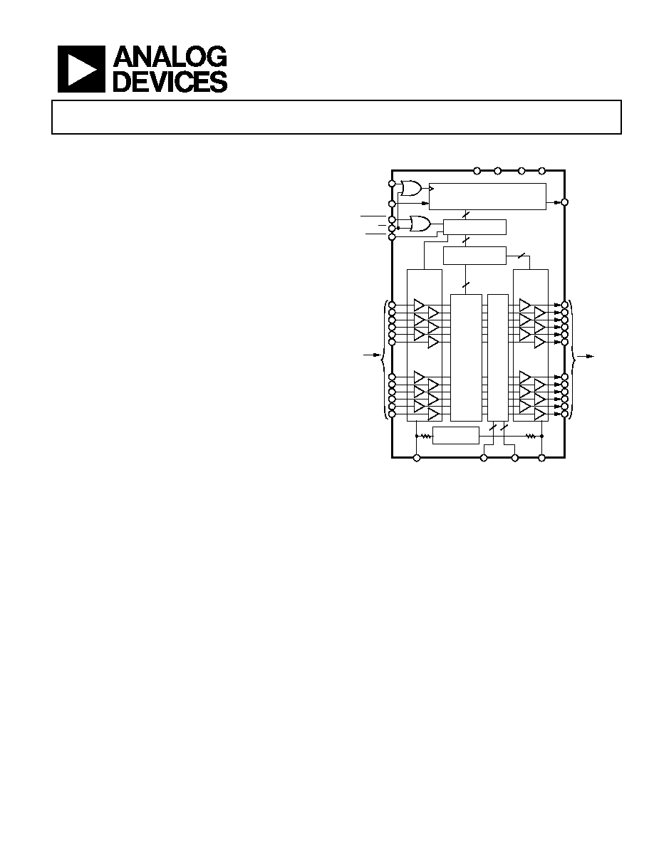
FUNCTIONAL BLOCK DIAGRAM
DGND
DVCC
VNEG
VPOS
DATA
OUT
ENABLE/
DISABLE
193-BIT SHIFT REGISTER
PARALLEL LATCH
32 × 5:32
DECODERS
ADV3200
(ADV3201)
OUTPUT
BUFFER
G = +1
(G = +2)
ENABLE/
BYPASS
32
193
192
1024
SYNC-TIP
CLAMP
SWITCH
MATRIX
OSD
MUX
32
OUTPUTS
32
INPUTS
..
.
..
.
..
.
..
.
32
REFERENCE
CLK
DATA IN
VCLAMP
VREF
OSD
INPUTS
OSD
SWITCHES
07
17
6-
0
01
UPDATE
CS
RESET
Figure 1.
GENERAL DESCRIPTION
The ADV3200/ADV3201 are 32 × 32 analog crosspoint switch
matrices. They feature a selectable sync-tip clamp input for
ac-coupled applications and an on-screen display (OSD)
insertion mux. With 48 dB of crosstalk and 80 dB isolation
at 5 MHz, the ADV3200/ADV3201 are useful in many high
density routing applications. The 0.1 dB flatness out to 60 MHz
makes the ADV3200/ADV3201 ideal for composite video
switching.
The 32 independent output buffers of the ADV3200/ADV3201
can be placed into a high impedance state for paralleling cross-
point outputs so that off channels present minimal loading to
an output bus if building a larger array. The part is available
in a gain of +1 (ADV3200) or +2 (ADV3201) for ease of use in
back-terminated load applications. A single 5 V supply, dual
±2.5 V supplies, or dual ±3.3 V supplies (G = +2) can be used
while consuming only 250 mA of idle current with all outputs
enabled. The channel switching is performed via a double
buffered, serial digital control, which can accommodate daisy
chaining of several devices.
The ADV3200/ADV3201 are packaged in a 176-lead exposed
pad LQFP (24 mm × 24 mm) and are available over the
extended industrial temperature range of 40°C to +85°C.
相关PDF资料 |
PDF描述 |
|---|---|
| ADV3203ASWZ | IC CROSSPOINT SWIT 32X16 176LQFP |
| ADV3205JSTZ | IC CROSSPOINT SWIT 16X16 100LQFP |
| ADV3220ACPZ-R7 | IC MULTIPLEXER 2:1 16LFCSP |
| ADV3222ARZ-R7 | IC MULTIPLEXER 4:1 16SOIC |
| ADV3225ACPZ | IC CROSSPOINT SW 16X8 72LFCSP |
相关代理商/技术参数 |
参数描述 |
|---|---|
| ADV3200-EVALZ | 功能描述:ADV3200 - Interface, Crosspoint Switch/Multiplexer Evaluation Board 制造商:analog devices inc. 系列:- 零件状态:有效 主要用途:接口,交叉点开关/多路复用器 嵌入式:- 使用的 IC/零件:ADV3200 主要属性:32 x 32 视频交叉点开关 辅助属性:图形用户界面 所含物品:板,线缆 标准包装:1 |
| ADV3201 | 制造商:AD 制造商全称:Analog Devices 功能描述:300 MHz, 32 × 32 Buffered Analog Crosspoint Switch |
| ADV3201ASWZ | 功能描述:IC CROSSPOINT SWIT 32X32 176LQFP RoHS:是 类别:集成电路 (IC) >> 接口 - 模拟开关,多路复用器,多路分解器 系列:- 应用说明:Ultrasound Imaging Systems Application Note 产品培训模块:Lead (SnPb) Finish for COTS Obsolescence Mitigation Program 标准包装:250 系列:- 功能:开关 电路:单刀单掷 导通状态电阻:48 欧姆 电压电源:单电源 电压 - 电源,单路/双路(±):2.7 V ~ 5.5 V 电流 - 电源:5µA 工作温度:0°C ~ 70°C 安装类型:表面贴装 封装/外壳:48-LQFP 供应商设备封装:48-LQFP(7x7) 包装:托盘 |
| ADV3201-EVALZ | 功能描述:ADV3201 - Interface, Crosspoint Switch/Multiplexer Evaluation Board 制造商:analog devices inc. 系列:- 零件状态:有效 主要用途:接口,交叉点开关/多路复用器 嵌入式:- 使用的 IC/零件:ADV3201 主要属性:32 x 32 视频交叉点开关 辅助属性:图形用户界面 所含物品:板,线缆 标准包装:1 |
| ADV3202 | 制造商:AD 制造商全称:Analog Devices 功能描述:300 MHz, 32 × 16 Buffered Analog Crosspoint Switch |
发布紧急采购,3分钟左右您将得到回复。