参数资料
| 型号: | ADV3200ASWZ |
| 厂商: | Analog Devices Inc |
| 文件页数: | 20/36页 |
| 文件大小: | 0K |
| 描述: | IC CROSSPOINT SWIT 32X32 176LQFP |
| 标准包装: | 1 |
| 功能: | 交叉点开关 |
| 电路: | 1 x 32:32 |
| 电压电源: | 单/双电源 |
| 电压 - 电源,单路/双路(±): | 5V,±2.5V,±3.3V |
| 电流 - 电源: | 250mA |
| 工作温度: | -40°C ~ 85°C |
| 安装类型: | 表面贴装 |
| 封装/外壳: | 176-LQFP |
| 供应商设备封装: | 176-LQFP-EP(24x24) |
| 包装: | 托盘 |
第1页第2页第3页第4页第5页第6页第7页第8页第9页第10页第11页第12页第13页第14页第15页第16页第17页第18页第19页当前第20页第21页第22页第23页第24页第25页第26页第27页第28页第29页第30页第31页第32页第33页第34页第35页第36页
ADV3200/ADV3201
Rev. 0 | Page 27 of
36
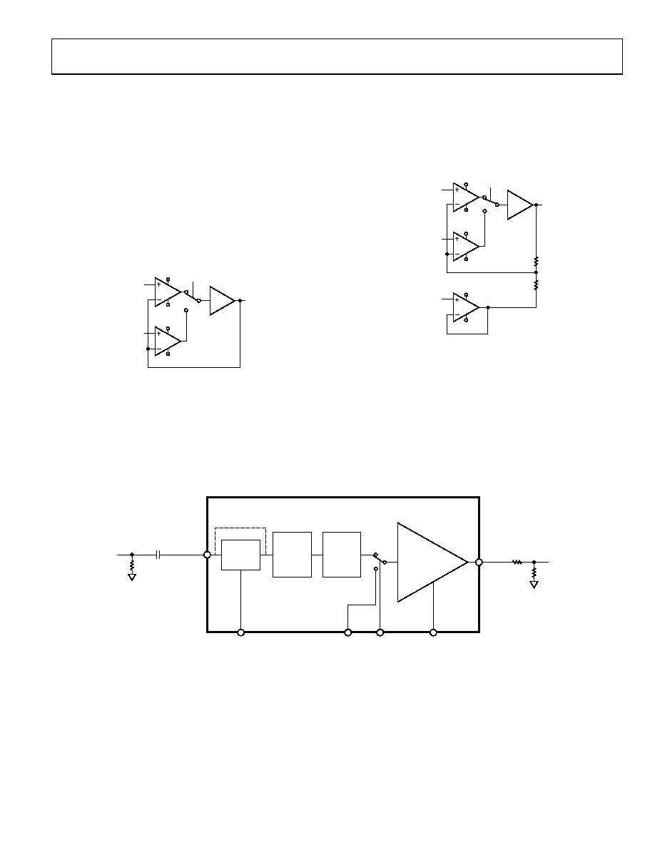
THEORY OF OPERATION
The ADV3200/ADV3201 are single-ended crosspoint arrays
with 32 outputs, each of which can be connected to any one
of 32 inputs. Thirty-two switchable input stages are connected
to each output buffer to form 32-to-1 multiplexers. There are 32
of these multiplexers, each with its inputs wired in parallel, for a
total array of 1024 stages forming a multicast-capable crosspoint
switch (see Figure 97).
In addition to connecting to any of the nominal inputs (INxx),
each output can also be connected to an associated OSDxx input
through an additional 2-to-1 multiplexer at each output. This
2-to-1 multiplexer switches between the output of the 32-to-1
multiplexer and the OSDxx input.
x1
OUT00
VPOS
VNEG
FROM INPUT
STAGES
VPOS
VNEG
OSD00
OSDS00
07
17
6-
00
6
Figure 95. Conceptual Diagram of Single Output Channel, G = +1 (ADV3200)
Decoding logic for each output selects one (or none) of the
input stages to drive the output stage. The enabled input stage
drives the output stage, which is configured as a unity-gain
amplifier in the ADV3200 (see Figure 95).
In the ADV3201, an internal resistive feedback network and
reference buffer provide for a total output stage gain of +2 (see
Figure 96). The input voltage to the reference buffer is the
VREF pin. This voltage is common to the entire chip and needs
to be driven from a low impedance source to avoid crosstalk.
OUT00
x1
VPOS
VNEG
FROM INPUT
STAGES
VPOS
VNEG
VREF
VPOS
VNEG
OSD00
OSDS00
2k
07
17
6-
0
07
Figure 96. Conceptual Diagram of Single Output Channel, G = +2 (ADV3201)
Each input to the ADV3200/ADV3201 is buffered by a receiver.
This receiver provides overvoltage protection for the input
stages by limiting signal swing. In the ADV3200, the output
of the receiver is limited to ±1.2 V about VREF, whereas in the
ADV3201, the signal swing is limited to ±1.2 V about midsupply.
This receiver is configured as a voltage feedback unity-gain
amplifier. Excess loop gain bandwidth product reduces the
effect of the closed-loop gain on the bandwidth of the device.
SWITCH
MATRIX
SYNC-TIP
CLAMP
RECEIVER
INxx
GND
OPTIONAL
AC COUPLING
CAPACITOR
75
OUTxx 75
75
ADV3200/ADV3201
VREF
OSDxx
OSDSxx
VCLAMP
BYPASS SYNC-TIP
CLAMP
07
17
6-
11
0
OUTPUT
BUFFER
G = +1 (ADV3200)
G = +2 (ADV3201)
Figure 97. ADV3200/ADV3201 Signal Chain (Single I/O Path)
相关PDF资料 |
PDF描述 |
|---|---|
| ADV3203ASWZ | IC CROSSPOINT SWIT 32X16 176LQFP |
| ADV3205JSTZ | IC CROSSPOINT SWIT 16X16 100LQFP |
| ADV3220ACPZ-R7 | IC MULTIPLEXER 2:1 16LFCSP |
| ADV3222ARZ-R7 | IC MULTIPLEXER 4:1 16SOIC |
| ADV3225ACPZ | IC CROSSPOINT SW 16X8 72LFCSP |
相关代理商/技术参数 |
参数描述 |
|---|---|
| ADV3200-EVALZ | 功能描述:ADV3200 - Interface, Crosspoint Switch/Multiplexer Evaluation Board 制造商:analog devices inc. 系列:- 零件状态:有效 主要用途:接口,交叉点开关/多路复用器 嵌入式:- 使用的 IC/零件:ADV3200 主要属性:32 x 32 视频交叉点开关 辅助属性:图形用户界面 所含物品:板,线缆 标准包装:1 |
| ADV3201 | 制造商:AD 制造商全称:Analog Devices 功能描述:300 MHz, 32 × 32 Buffered Analog Crosspoint Switch |
| ADV3201ASWZ | 功能描述:IC CROSSPOINT SWIT 32X32 176LQFP RoHS:是 类别:集成电路 (IC) >> 接口 - 模拟开关,多路复用器,多路分解器 系列:- 应用说明:Ultrasound Imaging Systems Application Note 产品培训模块:Lead (SnPb) Finish for COTS Obsolescence Mitigation Program 标准包装:250 系列:- 功能:开关 电路:单刀单掷 导通状态电阻:48 欧姆 电压电源:单电源 电压 - 电源,单路/双路(±):2.7 V ~ 5.5 V 电流 - 电源:5µA 工作温度:0°C ~ 70°C 安装类型:表面贴装 封装/外壳:48-LQFP 供应商设备封装:48-LQFP(7x7) 包装:托盘 |
| ADV3201-EVALZ | 功能描述:ADV3201 - Interface, Crosspoint Switch/Multiplexer Evaluation Board 制造商:analog devices inc. 系列:- 零件状态:有效 主要用途:接口,交叉点开关/多路复用器 嵌入式:- 使用的 IC/零件:ADV3201 主要属性:32 x 32 视频交叉点开关 辅助属性:图形用户界面 所含物品:板,线缆 标准包装:1 |
| ADV3202 | 制造商:AD 制造商全称:Analog Devices 功能描述:300 MHz, 32 × 16 Buffered Analog Crosspoint Switch |
发布紧急采购,3分钟左右您将得到回复。