参数资料
| 型号: | ADV601LCJSTZ |
| 厂商: | Analog Devices Inc |
| 文件页数: | 26/44页 |
| 文件大小: | 0K |
| 描述: | IC CODEC VIDEO DSP/SRL 120LQFP |
| 标准包装: | 1 |
| 类型: | 视频编解码器 |
| 数据接口: | DSP,串行 |
| 分辨率(位): | 8 b |
| 三角积分调变: | 无 |
| 电压 - 电源,模拟: | 4.5 V ~ 5.5 V |
| 电压 - 电源,数字: | 4.5 V ~ 5.5 V |
| 工作温度: | 0°C ~ 70°C |
| 安装类型: | 表面贴装 |
| 封装/外壳: | 120-LQFP |
| 供应商设备封装: | 120-LQFP(14x14) |
| 包装: | 托盘 |
第1页第2页第3页第4页第5页第6页第7页第8页第9页第10页第11页第12页第13页第14页第15页第16页第17页第18页第19页第20页第21页第22页第23页第24页第25页当前第26页第27页第28页第29页第30页第31页第32页第33页第34页第35页第36页第37页第38页第39页第40页第41页第42页第43页第44页
ADV601LC
–32–
REV. 0
TIMING PARAMETERS
This section contains signal timing information for the ADV601LC. Timing descriptions for the following items appear in this
section:
Clock signal timing
Video data transfer timing (CCIR-656, and Multiplexed Philips formats)
Host data transfer timing (direct register read/write access)
Clock Signal Timing
The diagram in this section shows timing for VCLK input and VCLKO output. All output values assume a maximum pin
loading of 50 pF.
Table XVIII. Video Clock Period, Frequency, Drift and Jitter
Min VCLK_CYC
Nominal VCLK_CYC
Max VCLK_CYC
Video Format
Period
Period (Frequency)
Period
1, 2
CCIR-601 PAL
35.2 ns
37 ns (27 MHz)
38.9 ns
CCIR-601 NTSC
35.2 ns
37 ns (27 MHz)
38.9 ns
NOTES
1VCLK Period Drift =
± 0.1 (VCLK_CYC/field.
2VCLK edge-to-edge jitter = 1 ns.
Table XIX. Video Clock Duty Cycle
Min
Nominal
Max
VCLK Duty Cycle
1
(40%)
(50%)
(60%)
NOTE
1VCLK Duty Cycle = t
VCLK_HI/(tVCLK_LO) × 100.
Table XX. Video Clock Timing Parameters
Parameter
Description
Min
Max
Unit
tVCLK_CYC
VCLK Signal, Cycle Time (1/Frequency) at 27 MHz
(See Video Clock Period Table)
tVCLKO_D0
VCLKO Signal, Delay (when VCLK2 = 0) at 27 MHz
10
29
ns
tVCLKO_D1
VCLKO Signal, Delay (when VCLK2 = 1) at 27 MHz
10
29
ns
TEST CONDITIONS
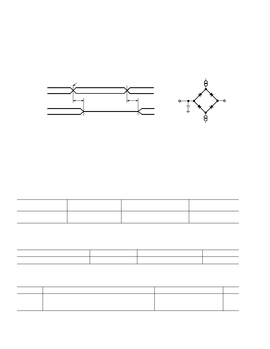
Figure 18 shows test condition voltage reference and device
loading information. These test conditions consider an output
as disabled when the output stops driving and goes from the
measured high or low voltage to a high impedance state. Tests
measure output disable time (tDISABLE) as the time between the
reference input signal crossing +1.5 V and the time that the
output reaches the high impedance state (also +1.5 V). Simi-
larly, these tests conditions consider an output as enabled when
the output leaves the high impedance state and begins driving a
measured high or low voltage. Tests measure output enable time
(tENABLE) as the time between the reference input signal crossing
+1.5 V and the time that the output reaches the measured high
or low voltage.
INPUT
REFERENCE
SIGNAL
OUTPUT
SIGNAL
t
DISABLED
t
ENABLED
1.5V
VOH
VOL
VIH
VIL
1.5V
INPUT & OUTPUT VOLTAGE/TIMING REFERENCES
DEVICE LOADING FOR AC MEASUREMENTS
TO
OUTPUT
PIN
2pF
+1.5V
IOL
IOH
Figure 18. Test Condition Voltage Reference and Device Loading
相关PDF资料 |
PDF描述 |
|---|---|
| ADV611JSTZ | IC CCTV DGTL VIDEO CODEC 120LQFP |
| ADV7120KPZ30 | IC DAC VIDEO 3CH 30MHZ 44PLCC |
| ADV7125WBCPZ170 | IC DAC VIDEO 3-CH 330MHZ 48VFQFN |
| ADV7171KSZ-REEL | IC DAC VIDEO ENC NTSC 44-MQFP |
| ADV7172KSTZ-REEL | IC DAC VIDEO NTSC 6-CH 48-LQFP |
相关代理商/技术参数 |
参数描述 |
|---|---|
| ADV601LCJSTZRL | 功能描述:IC CODEC VIDEO DSP/SRL 120LQFP RoHS:是 类别:集成电路 (IC) >> 接口 - 编解码器 系列:- 标准包装:2,500 系列:- 类型:立体声音频 数据接口:串行 分辨率(位):18 b ADC / DAC 数量:2 / 2 三角积分调变:是 S/N 比,标准 ADC / DAC (db):81.5 / 88 动态范围,标准 ADC / DAC (db):82 / 87.5 电压 - 电源,模拟:2.6 V ~ 3.3 V 电压 - 电源,数字:1.7 V ~ 3.3 V 工作温度:-40°C ~ 85°C 安装类型:表面贴装 封装/外壳:48-WFQFN 裸露焊盘 供应商设备封装:48-TQFN-EP(7x7) 包装:带卷 (TR) |
| ADV601LC-VIDEOPIPE | 制造商:Analog Devices 功能描述:TOOLS:DEVELOPMENT BOARDS H/W 制造商:Analog Devices 功能描述:EVALUATION BOARD ((NS)) |
| ADV601XS | 制造商:Analog Devices 功能描述: |
| ADV611 | 制造商:AD 制造商全称:Analog Devices 功能描述:CLOSED CIRCUIT TV DIGITAL VIDEO CODEC |
| ADV611JST | 制造商:Analog Devices 功能描述:Video Compression 120-Pin LQFP 制造商:Rochester Electronics LLC 功能描述:CLOSED CIRCUIT TV VIDEO CODEC - TQFP PKG - Tape and Reel |
发布紧急采购,3分钟左右您将得到回复。