- 您现在的位置:买卖IC网 > PDF目录10747 > AFE7222IRGCR (Texas Instruments)IC AFE 12BIT 65/130MSPS 64VQFN PDF资料下载
参数资料
| 型号: | AFE7222IRGCR |
| 厂商: | Texas Instruments |
| 文件页数: | 14/106页 |
| 文件大小: | 0K |
| 描述: | IC AFE 12BIT 65/130MSPS 64VQFN |
| 标准包装: | 2,000 |
| 位数: | 12 |
| 通道数: | 4 |
| 功率(瓦特): | 610mW |
| 电压 - 电源,模拟: | 2.85 V ~ 3.6 V |
| 电压 - 电源,数字: | 1.7 V ~ 1.9 V |
| 封装/外壳: | 64-VFQFN 裸露焊盘 |
| 供应商设备封装: | 64-VQFN 裸露焊盘(9x9) |
| 包装: | 带卷 (TR) |
第1页第2页第3页第4页第5页第6页第7页第8页第9页第10页第11页第12页第13页当前第14页第15页第16页第17页第18页第19页第20页第21页第22页第23页第24页第25页第26页第27页第28页第29页第30页第31页第32页第33页第34页第35页第36页第37页第38页第39页第40页第41页第42页第43页第44页第45页第46页第47页第48页第49页第50页第51页第52页第53页第54页第55页第56页第57页第58页第59页第60页第61页第62页第63页第64页第65页第66页第67页第68页第69页第70页第71页第72页第73页第74页第75页第76页第77页第78页第79页第80页第81页第82页第83页第84页第85页第86页第87页第88页第89页第90页第91页第92页第93页第94页第95页第96页第97页第98页第99页第100页第101页第102页第103页第104页第105页第106页
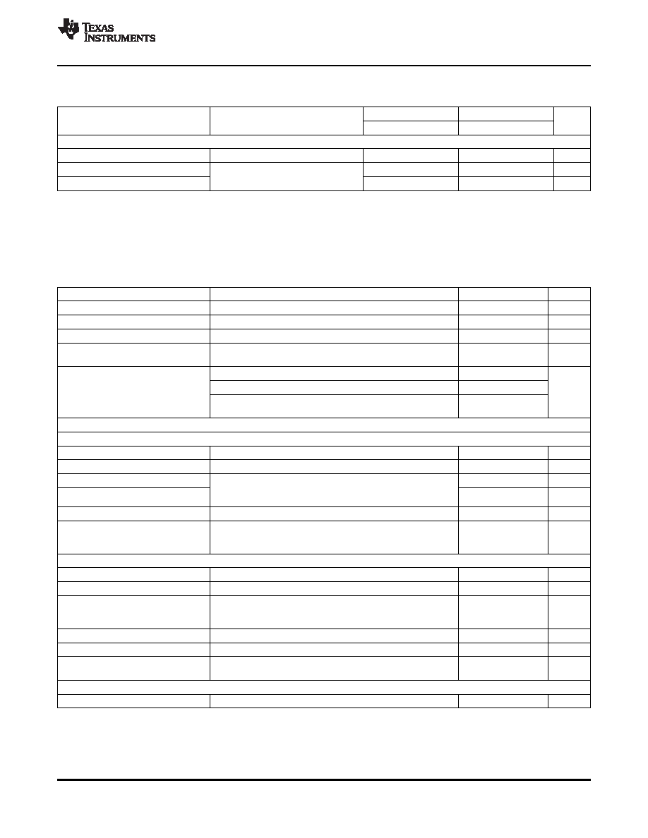
SLOS711B – NOVEMBER 2011 – REVISED MARCH 2012
3.11
TIMING REQUIREMENTS
Typical values at TA = 25°C, full temperature range is TMIN = –40°C to TMAX = 85°C, unless otherwise noted.
AFE7222
AFE7225
PARAMETER
TEST CONDITIONS
UNIT
MIN
TYP
MAX
MIN
TYP
MAX
SCLK INPUT
tSCLK
CLOCK period
25
ns
tSCLKH
CLOCK pulse width high
12.5
ns
Assuming 50/50 duty cycle
tSCLKL
CLOCK pulse width low
12.5
ns
3.12
TIMING REQUIREMENTS FOR RECEIVE PATH – LVDS AND CMOS MODES
Typical values are at 25°C, AVDD3_DAC = 3.0 V, AVDD3_AUX = 3.0 V, AVDD18_ADC = 1.8 V, DVDD18_CLK = 1.8 V,
DVDD18_DAC = 1.8 V, DVDD18 = 1.8 V, sampling frequency = 125 MSPS, sine wave input clock, 1.5 Vpp clock amplitude,
CLOAD = 5 pF
(1), R
LOAD = 100 Ω
(2), unless otherwise noted. Min and max values are across the full temperature range T
MIN = -
40°C to TMAX = 85°C, AVDD3_DAC = 3.0 V, AVDD3_AUX = 3.0 V, AVDD18_ADC = 1.8 V, DVDD18_CLK = 1.8 V,
DVDD18_DAC = 1.8 V, DVDD18 = 1.7 V to 1.9 V
PARAMETER
TEST CONDITIONS
MIN
TYP MAX
UNIT
TA
Aperture delay
2
ns
Aperture delay matching
Between two channels on the same device
±120
ps
Aperture delay matching
Between two devices at same temperature and DVDD18 supply
±450
ps
Jitter added by internal clock distribution, specified as it relates
TJ
Aperture jitter
250
fs rms
to the receive ADC
Default Mode
16
Mixer Enabled (RX_MIXER_EN = 1)
33
clock
ADC Latency(3)
cycles
RX QMC Gain Phase Correction Enabled
22
(RX_QMC_CORR_ENA=1, RX_QMC_CORR_ENB=1)
LVDS OUTPUT INTERFACE
2-WIRE MODE, DDR CLOCK(4), Sampling frequency = 125MSPS
tsu
Data setup time (5)
Data valid(5) to zero-crossing of CLKOUTP
0.29
0.42
ns
th
Data hold time (5)
Zero-crossing of CLKOUTP to data becoming invalid (5)
0.3
0.47
ns
tPDI
Clock propagation delay
Input clock rising edge cross-over to output clock rising edge
tPDI = tDELAY
ns
cross-over 10 MSPS
≤ Sampling frequency ≤ 125 MSPS Ts =
tdelay
11.5
13.8
15.5
ns
1/Sampling frequency
Variation of tdelay
Between two devices at same temperature and DVDD18 supply
±300
ps
Duty cycle of differential clock, (ADC_DCLKOUTP-
LVDS bit clock duty cycle
ADC_DCLKOUTM) 10 MSPS
≤ Sampling frequency ≤ 125
50%
MSPS
2-WIRE MODE, SDR CLOCK(4), Sampling frequency = 65MSPS
tsu
Data setup time (5)
Data valid (5) to zero-crossing of CLKOUTP
0.85
1.08
ns
th
Data hold time (5)
Zero-crossing of CLKOUTP to data becoming invalid (5)
1.08
1.21
ns
Input clock rising edge cross-over to output clock rising edge
tPDI
Clock propagation delay
cross-over 10 MSPS
≤ Sampling frequency ≤ 65 MSPS Ts =
tPDI = 0.5*Ts + tDELAY
ns
1/Sampling frequency
tdelay
11.5
14
16.5
ns
Variation of tdelay
Between two devices at same temperature and DVDD18 supply
±300
ps
Duty cycle of differential clock, (CLKOUTP-CLKOUTM) 10
LVDS bit clock duty cycle
50%
MSPS
≤ Sampling frequency ≤ 65 MSPS
1-WIRE MODE (DDR CLOCK ONLY)(4), Sampling frequency = 65MSPS
tsu
Data setup time (5)
Data valid (5) to zero-crossing of CLKOUTP
0.25
0.39
ns
(1)
CLOAD is the effective external single-ended load capacitance between each output pin and ground
(2)
RLOAD is the differential load resistance between the LVDS output pair.
(3)
At higher frequencies, tPDI is greater than one clock period and overall latency = ADC latency + 1.
(4)
Measurements are done with a transmission line of 100-
Ω characteristic impedance between the device and the load. Setup and hold
time specifications take into account the effect of jitter on the output data and clock.
(5)
Data valid refers to LOGIC HIGH of +100.0 mV and LOGIC LOW of -100.0 mV.
Copyright 2011–2012, Texas Instruments Incorporated
ELECTRICAL SPECIFICATIONS
15
相关PDF资料 |
PDF描述 |
|---|---|
| JKXFD0G07MSSDPGR | CONN PLUG 7POS CABLE PIN SLD |
| VE-B3W-IV | CONVERTER MOD DC/DC 5.5V 150W |
| VE-B3T-IV | CONVERTER MOD DC/DC 6.5V 150W |
| VI-J3L-MY-F2 | CONVERTER MOD DC/DC 28V 50W |
| VI-B6V-MX-F1 | CONVERTER MOD DC/DC 5.8V 75W |
相关代理商/技术参数 |
参数描述 |
|---|---|
| AFE7222IRGCT | 功能描述:射频前端 Dual 12B,65MSPS ADC RoHS:否 制造商:Skyworks Solutions, Inc. 类型: 工作频率:2.4 GHz, 5 GHz 最大数据速率:54 Mbps 噪声系数: 工作电源电压:3.3 V 电源电流:180 mA 最大工作温度:+ 85 C 安装风格:SMD/SMT 封装 / 箱体:QFN-32 |
| AFE7225 | 制造商:TI 制造商全称:Texas Instruments 功能描述:Analog Front End Wideband Mixed-Signal Transceiver |
| AFE7225EVM | 功能描述:射频开发工具 AFE7225 Eval Mod RoHS:否 制造商:Taiyo Yuden 产品:Wireless Modules 类型:Wireless Audio 工具用于评估:WYSAAVDX7 频率: 工作电源电压:3.4 V to 5.5 V |
| AFE7225IRGC25 | 功能描述:射频前端 Dual 12B,125MSPS ADC RoHS:否 制造商:Skyworks Solutions, Inc. 类型: 工作频率:2.4 GHz, 5 GHz 最大数据速率:54 Mbps 噪声系数: 工作电源电压:3.3 V 电源电流:180 mA 最大工作温度:+ 85 C 安装风格:SMD/SMT 封装 / 箱体:QFN-32 |
| AFE7225IRGCR | 功能描述:射频前端 Dual 12B,125MSPS ADC RoHS:否 制造商:Skyworks Solutions, Inc. 类型: 工作频率:2.4 GHz, 5 GHz 最大数据速率:54 Mbps 噪声系数: 工作电源电压:3.3 V 电源电流:180 mA 最大工作温度:+ 85 C 安装风格:SMD/SMT 封装 / 箱体:QFN-32 |
发布紧急采购,3分钟左右您将得到回复。