- 您现在的位置:买卖IC网 > PDF目录10747 > AFE7222IRGCR (Texas Instruments)IC AFE 12BIT 65/130MSPS 64VQFN PDF资料下载
参数资料
| 型号: | AFE7222IRGCR |
| 厂商: | Texas Instruments |
| 文件页数: | 94/106页 |
| 文件大小: | 0K |
| 描述: | IC AFE 12BIT 65/130MSPS 64VQFN |
| 标准包装: | 2,000 |
| 位数: | 12 |
| 通道数: | 4 |
| 功率(瓦特): | 610mW |
| 电压 - 电源,模拟: | 2.85 V ~ 3.6 V |
| 电压 - 电源,数字: | 1.7 V ~ 1.9 V |
| 封装/外壳: | 64-VFQFN 裸露焊盘 |
| 供应商设备封装: | 64-VQFN 裸露焊盘(9x9) |
| 包装: | 带卷 (TR) |
第1页第2页第3页第4页第5页第6页第7页第8页第9页第10页第11页第12页第13页第14页第15页第16页第17页第18页第19页第20页第21页第22页第23页第24页第25页第26页第27页第28页第29页第30页第31页第32页第33页第34页第35页第36页第37页第38页第39页第40页第41页第42页第43页第44页第45页第46页第47页第48页第49页第50页第51页第52页第53页第54页第55页第56页第57页第58页第59页第60页第61页第62页第63页第64页第65页第66页第67页第68页第69页第70页第71页第72页第73页第74页第75页第76页第77页第78页第79页第80页第81页第82页第83页第84页第85页第86页第87页第88页第89页第90页第91页第92页第93页当前第94页第95页第96页第97页第98页第99页第100页第101页第102页第103页第104页第105页第106页
CLKINP
CLKINN
Clock
Divider
%1,2,4
Clock
Divider
%1,2,4
PLL
X2,4
ADC_CLK
DAC_CLK
MUX
PLL_ENABLE
REG_SE_CLK
DIV_ADC<1:0>
DIV_DAC<1:0>
DCC
(Duty Cycle
Correction)
MUX
ENABLE_DCC
Single-
ended
Buffer
Single-
ended
Buffer
Differential
Buffer
SLOS711B – NOVEMBER 2011 – REVISED MARCH 2012
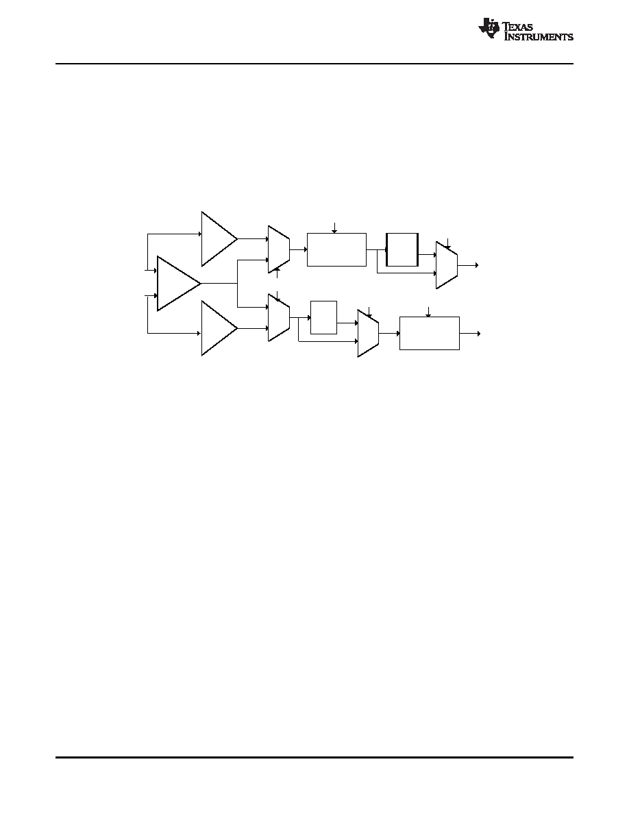
10.7.2 CLOCKING
The clock inputs are versatile. The AFE7225/7222 can be driven by a differential clock, a single-ended
clock or two independent single-ended clocks. Low voltage CMOS for single-ended and LVDS for
differential are supported clock levels. Since routing single-ended clocks on the printed circuit board is
different from system to system, it is possible to see some performance degradation in the data converters
if the clock becomes corrupted prior to entering the AFE7225/7222. This is less likely to occur if using a
differential clock routed on the board due to the common-mode noise rejection of the differential clock
receiver.
The full block diagram of the clocking to the ADC and DAC is shown below.
Figure 10-13. Clocking
Depending on the ADC input frequency and the target SNR of the receiver, it may be important to provide
a low jitter clock source to the AFE7225/7222. A good estimate for required clock jitter to achieve a certain
SNR can be found using SNR = 20*log10(2*pi*FINadc *JITTERtotal). The JITTERtotal is the rms
summation of the external clock jitter and the internal AFE7225/7222 RX ADC clocking aperture jitter,
specified in the timing characteristics table. A good target for the total jitter is a value that allows an SNR
that meets or exceeds the ADC SNR so that the clock source jitter will not degrade the SNR. Note that the
SNR is dependent on the analog input frequency and not the clock frequency.
When different rate clocks are required for the ADC and the DAC (for example, DAC_CLK is 2X rate of
ADC_CLK), it is strongly recommended that the input clock be at the higher of the two rates. Dividing the
high speed clock to derive the half rate clock always gives much lower jitter than using the PLL to multiply
the lower rate clock to derive the higher rate inside the chip. Use the PLL only when performance
requirements are relaxed and the additional jitter is tolerable (usually when the analog I/O frequencies are
low).
The equivalent circuit model of the differential buffer is shown below. Note that even with the single ended
buffer is enabled, the loading from the passive components in the differential buffer circuit (including the 2
pF differential cap, the two 5 kOhm resistors and the equivalent input load, Ceq are still present).
88
DIGITAL INTERFACE
Copyright 2011–2012, Texas Instruments Incorporated
相关PDF资料 |
PDF描述 |
|---|---|
| JKXFD0G07MSSDPGR | CONN PLUG 7POS CABLE PIN SLD |
| VE-B3W-IV | CONVERTER MOD DC/DC 5.5V 150W |
| VE-B3T-IV | CONVERTER MOD DC/DC 6.5V 150W |
| VI-J3L-MY-F2 | CONVERTER MOD DC/DC 28V 50W |
| VI-B6V-MX-F1 | CONVERTER MOD DC/DC 5.8V 75W |
相关代理商/技术参数 |
参数描述 |
|---|---|
| AFE7222IRGCT | 功能描述:射频前端 Dual 12B,65MSPS ADC RoHS:否 制造商:Skyworks Solutions, Inc. 类型: 工作频率:2.4 GHz, 5 GHz 最大数据速率:54 Mbps 噪声系数: 工作电源电压:3.3 V 电源电流:180 mA 最大工作温度:+ 85 C 安装风格:SMD/SMT 封装 / 箱体:QFN-32 |
| AFE7225 | 制造商:TI 制造商全称:Texas Instruments 功能描述:Analog Front End Wideband Mixed-Signal Transceiver |
| AFE7225EVM | 功能描述:射频开发工具 AFE7225 Eval Mod RoHS:否 制造商:Taiyo Yuden 产品:Wireless Modules 类型:Wireless Audio 工具用于评估:WYSAAVDX7 频率: 工作电源电压:3.4 V to 5.5 V |
| AFE7225IRGC25 | 功能描述:射频前端 Dual 12B,125MSPS ADC RoHS:否 制造商:Skyworks Solutions, Inc. 类型: 工作频率:2.4 GHz, 5 GHz 最大数据速率:54 Mbps 噪声系数: 工作电源电压:3.3 V 电源电流:180 mA 最大工作温度:+ 85 C 安装风格:SMD/SMT 封装 / 箱体:QFN-32 |
| AFE7225IRGCR | 功能描述:射频前端 Dual 12B,125MSPS ADC RoHS:否 制造商:Skyworks Solutions, Inc. 类型: 工作频率:2.4 GHz, 5 GHz 最大数据速率:54 Mbps 噪声系数: 工作电源电压:3.3 V 电源电流:180 mA 最大工作温度:+ 85 C 安装风格:SMD/SMT 封装 / 箱体:QFN-32 |
发布紧急采购,3分钟左右您将得到回复。