- 您现在的位置:买卖IC网 > PDF目录294983 > AGLN030V2-ZCSG81 FPGA, 768 CLBS, 30000 GATES, 250 MHz, PBGA81 PDF资料下载
参数资料
| 型号: | AGLN030V2-ZCSG81 |
| 元件分类: | FPGA |
| 英文描述: | FPGA, 768 CLBS, 30000 GATES, 250 MHz, PBGA81 |
| 封装: | 5 X 5 MM, 0.8 MM HEIGHT, 0.5 MM PITCH, GREEN, CSP-81 |
| 文件页数: | 1/140页 |
| 文件大小: | 4325K |
| 代理商: | AGLN030V2-ZCSG81 |
当前第1页第2页第3页第4页第5页第6页第7页第8页第9页第10页第11页第12页第13页第14页第15页第16页第17页第18页第19页第20页第21页第22页第23页第24页第25页第26页第27页第28页第29页第30页第31页第32页第33页第34页第35页第36页第37页第38页第39页第40页第41页第42页第43页第44页第45页第46页第47页第48页第49页第50页第51页第52页第53页第54页第55页第56页第57页第58页第59页第60页第61页第62页第63页第64页第65页第66页第67页第68页第69页第70页第71页第72页第73页第74页第75页第76页第77页第78页第79页第80页第81页第82页第83页第84页第85页第86页第87页第88页第89页第90页第91页第92页第93页第94页第95页第96页第97页第98页第99页第100页第101页第102页第103页第104页第105页第106页第107页第108页第109页第110页第111页第112页第113页第114页第115页第116页第117页第118页第119页第120页第121页第122页第123页第124页第125页第126页第127页第128页第129页第130页第131页第132页第133页第134页第135页第136页第137页第138页第139页第140页
April 2010
I
2010 Actel Corporation
IGLOO nano Low Power Flash FPGAs
with Flash*Freeze Technology
Features and Benefits
Low Power
nanoPower Consumption—Industry’s Lowest Power
1.2 V to 1.5 V Core Voltage Support for Low Power
Supports Single-Voltage System Operation
Low Power Active FPGA Operation
Flash*Freeze Technology Enables Ultra-Low Power
Consumption while Maintaining FPGA Content
Easy Entry to / Exit from Ultra-Low Power Flash*Freeze Mode
Small Footprint Packages
As Small as 3x3 mm in Size
Wide Range of Features
10,000 to 250,000 System Gates
Up to 36 kbits of True Dual-Port SRAM
Up to 71 User I/Os
Reprogrammable Flash Technology
130-nm, 7-Layer Metal, Flash-Based CMOS Process
Live-at-Power-Up (LAPU) Level 0 Support
Single-Chip Solution
Retains Programmed Design When Powered Off
250 MHz (1.5 V systems) and 160 MHz (1.2 V systems) System
Performance
In-System Programming (ISP) and Security
Secure ISP Using On-Chip 128-Bit Advanced Encryption
Standard (AES) Decryption via JTAG (IEEE 1532–compliant)
FlashLock to Secure FPGA Contents
1.2 V Programming
High-Performance Routing Hierarchy
Segmented, Hierarchical Routing and Clock Structure
Advanced I/Os
1.2 V, 1.5 V, 1.8 V, 2.5 V, and 3.3 V Mixed-Voltage Operation
Bank-Selectable I/O Voltages—up to 4 Banks per Chip
Single-Ended I/O Standards: LVTTL, LVCMOS
3.3V /2.5 V / 1.8V /1.5 V/1.2 V
Wide Range Power Supply Voltage Support per JESD8-B,
Allowing I/Os to Operate from 2.7 V to 3.6 V
Wide Range Power Supply Voltage Support per JESD8-12,
Allowing I/Os to Operate from 1.14 V to 1.575 V
I/O Registers on Input, Output, and Enable Paths
Selectable Schmitt Trigger Inputs
Hot-Swappable and Cold-Sparing I/Os
Programmable Output Slew Rate and Drive Strength
Weak Pull-Up/-Down
IEEE 1149.1 (JTAG) Boundary Scan Test
Pin-Compatible Packages across the IGLOO Family
Clock Conditioning Circuit (CCC) and PLL
Up to Six CCC Blocks, One with an Integrated PLL
Configurable Phase Shift, Multiply/Divide, Delay
Capabilities, and External Feedback
Wide Input Frequency Range (1.5 MHz up to 250 MHz)
Embedded Memory
1 kbit of FlashROM User Nonvolatile Memory
SRAMs and FIFOs with Variable-Aspect-Ratio 4,608-Bit RAM
Blocks (×1, ×2, ×4, ×9, and ×18 organizations)
True Dual-Port SRAM (except × 18 organization)
Enhanced Commercial Temperature Range
–20°C to +70°C
AGLN030 and smaller devices do not support this feature.
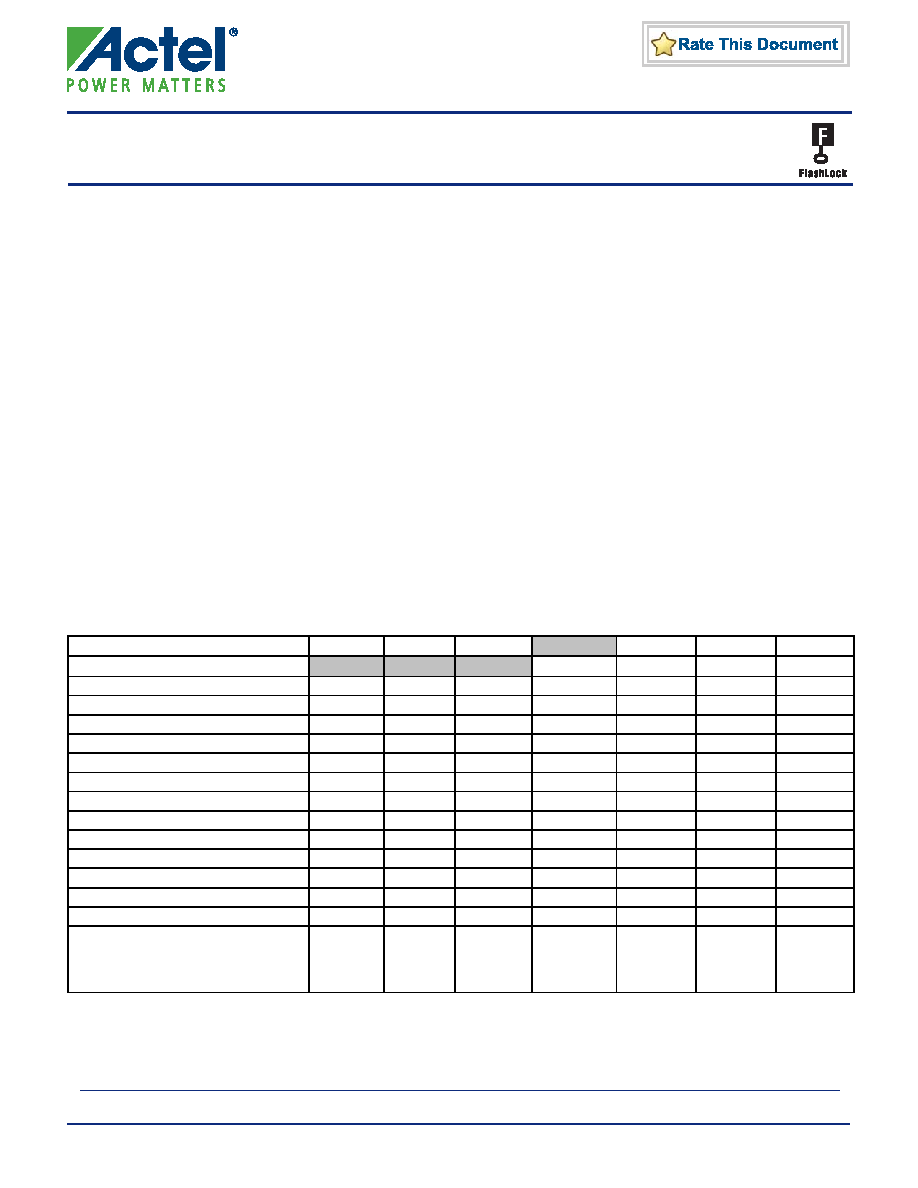
Table 1 IGLOO nano Devices
IGLOO nano Devices
AGLN010 AGLN015
AGLN020
AGLN060
AGLN125
AGLN250
IGLOO nano-Z Devices1
AGLN030Z1 AGLN060Z AGLN125Z AGLN250Z
System Gates
10K
15K
20K
30K
60K
125K
250K
Typical Equivalent Macrocells
86
128
172
256
512
1,024
2,048
VersaTiles (D-flip-flops)
260
384
520
768
1,536
3,072
6,144
Flash*Freeze Mode (typical, W)
2
4
5
10
16
24
RAM kbits (1,024 bits)2
–
18
36
4,608-Bit Blocks2
––
–
4
8
FlashROM Bits
1 k
Secure (AES) ISP2
–
Yes
Integrated PLL in CCCs 2,3
––
–
1
VersaNet Globals
4
6
18
I/O Banks
2
3
2
4
Maximum User I/Os (packaged device)
34
49
52
77
71
68
Maximum User I/Os (Known Good Die)
34
–
52
83
71
68
Package Pins
UC/CS
QFN
VQFP
UC36
QN48
QN68
UC81,
CS81
QN68
UC81, CS81
QN48, QN68
VQ100
CS81
VQ100
CS81
VQ100
CS81
VQ100
Notes:
1. AGLN030 is available in the Z feature grade only.
2. AGLN030 and smaller devices do not support this feature.
3. AGLN060, AGLN125, and AGLN250 in the CS81 package do not support PLLs.
4. For higher densities and support of additional features, refer to the IGLOO and IGLOOe handbooks.
Revision 10
相关PDF资料 |
PDF描述 |
|---|---|
| AGLN030V2-ZQN48I | FPGA, 768 CLBS, 30000 GATES, 250 MHz, QCC48 |
| AGLN030V2-ZQN48 | FPGA, 768 CLBS, 30000 GATES, 250 MHz, QCC48 |
| AGLN030V2-ZQN68I | FPGA, 768 CLBS, 30000 GATES, 250 MHz, QCC68 |
| AGLN030V2-ZQN68 | FPGA, 768 CLBS, 30000 GATES, 250 MHz, QCC68 |
| AGLN030V2-ZQNG48I | FPGA, 768 CLBS, 30000 GATES, 250 MHz, QCC48 |
相关代理商/技术参数 |
参数描述 |
|---|---|
| AGLN030V2-ZCSG81I | 功能描述:IC FPGA NANO 1KB 30K 81-CSP RoHS:是 类别:集成电路 (IC) >> 嵌入式 - FPGA(现场可编程门阵列) 系列:IGLOO nano 标准包装:152 系列:IGLOO PLUS LAB/CLB数:- 逻辑元件/单元数:792 RAM 位总计:- 输入/输出数:120 门数:30000 电源电压:1.14 V ~ 1.575 V 安装类型:表面贴装 工作温度:-40°C ~ 85°C 封装/外壳:289-TFBGA,CSBGA 供应商设备封装:289-CSP(14x14) |
| AGLN030V2-ZQNG48 | 功能描述:IC FPGA NANO 1KB 30K 48-QFN RoHS:是 类别:集成电路 (IC) >> 嵌入式 - FPGA(现场可编程门阵列) 系列:IGLOO nano 标准包装:152 系列:IGLOO PLUS LAB/CLB数:- 逻辑元件/单元数:792 RAM 位总计:- 输入/输出数:120 门数:30000 电源电压:1.14 V ~ 1.575 V 安装类型:表面贴装 工作温度:-40°C ~ 85°C 封装/外壳:289-TFBGA,CSBGA 供应商设备封装:289-CSP(14x14) |
| AGLN030V2-ZQNG48I | 功能描述:IC FPGA NANO 1KB 30K 48-QFN RoHS:是 类别:集成电路 (IC) >> 嵌入式 - FPGA(现场可编程门阵列) 系列:IGLOO nano 标准包装:152 系列:IGLOO PLUS LAB/CLB数:- 逻辑元件/单元数:792 RAM 位总计:- 输入/输出数:120 门数:30000 电源电压:1.14 V ~ 1.575 V 安装类型:表面贴装 工作温度:-40°C ~ 85°C 封装/外壳:289-TFBGA,CSBGA 供应商设备封装:289-CSP(14x14) |
| AGLN030V2-ZQNG68 | 功能描述:IC FPGA NANO 1KB 30K 68-QFN RoHS:是 类别:集成电路 (IC) >> 嵌入式 - FPGA(现场可编程门阵列) 系列:IGLOO nano 标准包装:152 系列:IGLOO PLUS LAB/CLB数:- 逻辑元件/单元数:792 RAM 位总计:- 输入/输出数:120 门数:30000 电源电压:1.14 V ~ 1.575 V 安装类型:表面贴装 工作温度:-40°C ~ 85°C 封装/外壳:289-TFBGA,CSBGA 供应商设备封装:289-CSP(14x14) |
| AGLN030V2-ZQNG68I | 功能描述:IC FPGA NANO 1KB 30K 68-QFN RoHS:是 类别:集成电路 (IC) >> 嵌入式 - FPGA(现场可编程门阵列) 系列:IGLOO nano 标准包装:152 系列:IGLOO PLUS LAB/CLB数:- 逻辑元件/单元数:792 RAM 位总计:- 输入/输出数:120 门数:30000 电源电压:1.14 V ~ 1.575 V 安装类型:表面贴装 工作温度:-40°C ~ 85°C 封装/外壳:289-TFBGA,CSBGA 供应商设备封装:289-CSP(14x14) |
发布紧急采购,3分钟左右您将得到回复。