参数资料
| 型号: | AM1808BZWT4 |
| 厂商: | Texas Instruments |
| 文件页数: | 261/264页 |
| 文件大小: | 0K |
| 描述: | IC ARM9 MPU 361NFBGA |
| 标准包装: | 90 |
| 系列: | ARM9 |
| 处理器类型: | ARM 微处理器 |
| 速度: | 456MHz |
| 电压: | 1.25 V ~ 1.35 V |
| 安装类型: | 表面贴装 |
| 封装/外壳: | 361-LFBGA |
| 供应商设备封装: | 361-NFBGA(16x16) |
| 包装: | 托盘 |
| 其它名称: | 296-28241 |
第1页第2页第3页第4页第5页第6页第7页第8页第9页第10页第11页第12页第13页第14页第15页第16页第17页第18页第19页第20页第21页第22页第23页第24页第25页第26页第27页第28页第29页第30页第31页第32页第33页第34页第35页第36页第37页第38页第39页第40页第41页第42页第43页第44页第45页第46页第47页第48页第49页第50页第51页第52页第53页第54页第55页第56页第57页第58页第59页第60页第61页第62页第63页第64页第65页第66页第67页第68页第69页第70页第71页第72页第73页第74页第75页第76页第77页第78页第79页第80页第81页第82页第83页第84页第85页第86页第87页第88页第89页第90页第91页第92页第93页第94页第95页第96页第97页第98页第99页第100页第101页第102页第103页第104页第105页第106页第107页第108页第109页第110页第111页第112页第113页第114页第115页第116页第117页第118页第119页第120页第121页第122页第123页第124页第125页第126页第127页第128页第129页第130页第131页第132页第133页第134页第135页第136页第137页第138页第139页第140页第141页第142页第143页第144页第145页第146页第147页第148页第149页第150页第151页第152页第153页第154页第155页第156页第157页第158页第159页第160页第161页第162页第163页第164页第165页第166页第167页第168页第169页第170页第171页第172页第173页第174页第175页第176页第177页第178页第179页第180页第181页第182页第183页第184页第185页第186页第187页第188页第189页第190页第191页第192页第193页第194页第195页第196页第197页第198页第199页第200页第201页第202页第203页第204页第205页第206页第207页第208页第209页第210页第211页第212页第213页第214页第215页第216页第217页第218页第219页第220页第221页第222页第223页第224页第225页第226页第227页第228页第229页第230页第231页第232页第233页第234页第235页第236页第237页第238页第239页第240页第241页第242页第243页第244页第245页第246页第247页第248页第249页第250页第251页第252页第253页第254页第255页第256页第257页第258页第259页第260页当前第261页第262页第263页第264页
SPRS653E – FEBRUARY 2010 – REVISED MARCH 2014
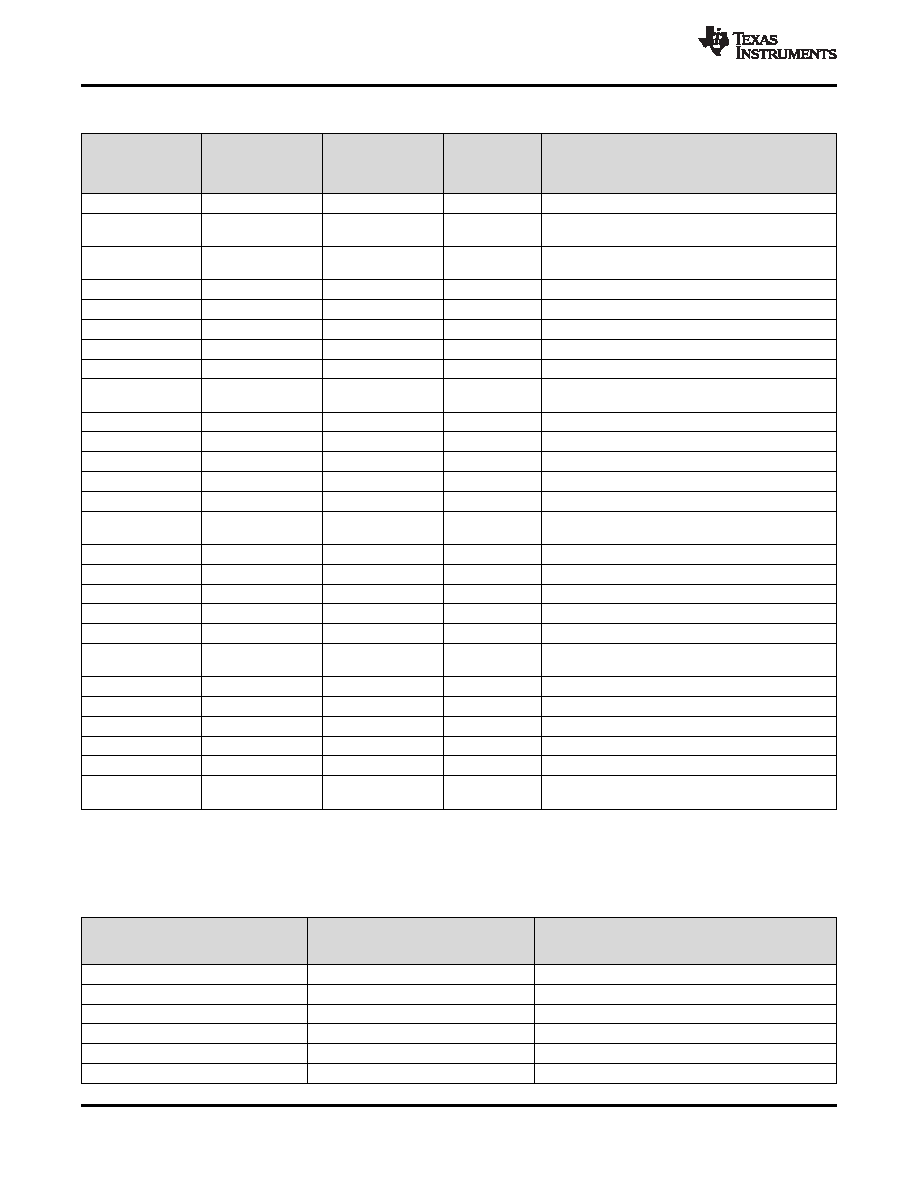
Table 6-11. EDMA3 Transfer Controller (EDMA3TC) Registers (continued)
EDMA0
EDMA1
ACRONYM
REGISTER DESCRIPTION
Transfer Controller
0
1
0
BYTE ADDRESS
0x01C0 8280
0x01C0 8680
0x01E3 8280
DFCNTRLD
Destination FIFO Set Count Reload Register
0x01C0 8284
0x01C0 8684
0x01E3 8284
DFSRCBREF
Destination FIFO Set Source Address B-Reference
Register
0x01C0 8288
0x01C0 8688
0x01E3 8288
DFDSTBREF
Destination FIFO Set Destination Address B-
Reference Register
0x01C0 8300
0x01C0 8700
0x01E3 8300
DFOPT0
Destination FIFO Options Register 0
0x01C0 8304
0x01C0 8704
0x01E3 8304
DFSRC0
Destination FIFO Source Address Register 0
0x01C0 8308
0x01C0 8708
0x01E3 8308
DFCNT0
Destination FIFO Count Register 0
0x01C0 830C
0x01C0 870C
0x01E3 830C
DFDST0
Destination FIFO Destination Address Register 0
0x01C0 8310
0x01C0 8710
0x01E3 8310
DFBIDX0
Destination FIFO B-Index Register 0
0x01C0 8314
0x01C0 8714
0x01E3 8314
DFMPPRXY0
Destination FIFO Memory Protection Proxy Register
0
0x01C0 8340
0x01C0 8740
0x01E3 8340
DFOPT1
Destination FIFO Options Register 1
0x01C0 8344
0x01C0 8744
0x01E3 8344
DFSRC1
Destination FIFO Source Address Register 1
0x01C0 8348
0x01C0 8748
0x01E3 8348
DFCNT1
Destination FIFO Count Register 1
0x01C0 834C
0x01C0 874C
0x01E3 834C
DFDST1
Destination FIFO Destination Address Register 1
0x01C0 8350
0x01C0 8750
0x01E3 8350
DFBIDX1
Destination FIFO B-Index Register 1
0x01C0 8354
0x01C0 8754
0x01E3 8354
DFMPPRXY1
Destination FIFO Memory Protection Proxy Register
1
0x01C0 8380
0x01C0 8780
0x01E3 8380
DFOPT2
Destination FIFO Options Register 2
0x01C0 8384
0x01C0 8784
0x01E3 8384
DFSRC2
Destination FIFO Source Address Register 2
0x01C0 8388
0x01C0 8788
0x01E3 8388
DFCNT2
Destination FIFO Count Register 2
0x01C0 838C
0x01C0 878C
0x01E3 838C
DFDST2
Destination FIFO Destination Address Register 2
0x01C0 8390
0x01C0 8790
0x01E3 8390
DFBIDX2
Destination FIFO B-Index Register 2
0x01C0 8394
0x01C0 8794
0x01E3 8394
DFMPPRXY2
Destination FIFO Memory Protection Proxy Register
2
0x01C0 83C0
0x01C0 87C0
0x01E3 83C0
DFOPT3
Destination FIFO Options Register 3
0x01C0 83C4
0x01C0 87C4
0x01E3 83C4
DFSRC3
Destination FIFO Source Address Register 3
0x01C0 83C8
0x01C0 87C8
0x01E3 83C8
DFCNT3
Destination FIFO Count Register 3
0x01C0 83CC
0x01C0 87CC
0x01E3 83CC
DFDST3
Destination FIFO Destination Address Register 3
0x01C0 83D0
0x01C0 87D0
0x01E3 83D0
DFBIDX3
Destination FIFO B-Index Register 3
0x01C0 83D4
0x01C0 87D4
0x01E3 83D4
DFMPPRXY3
Destination FIFO Memory Protection Proxy Register
3
Table 6-12 shows an abbreviation of the set of registers which make up the parameter set for each of 128
EDMA events. Each of the parameter register sets consist of 8 32-bit word entries. Table 6-13 shows the
parameter set entry registers with relative memory address locations within each of the parameter sets.
Table 6-12. EDMA Parameter Set RAM
EDMA0
EDMA1
Channel Controller 0
DESCRIPTION
BYTE ADDRESS RANGE
0x01C0 4000 - 0x01C0 401F
0x01E3 4000 - 0x01E3 401F
Parameters Set 0 (8 32-bit words)
0x01C0 4020 - 0x01C0 403F
0x01E3 4020 - 0x01E3 403F
Parameters Set 1 (8 32-bit words)
0x01C0 4040 - 0x01CC0 405F
0x01E3 4040 - 0x01CE3 405F
Parameters Set 2 (8 32-bit words)
0x01C0 4060 - 0x01C0 407F
0x01E3 4060 - 0x01E3 407F
Parameters Set 3 (8 32-bit words)
0x01C0 4080 - 0x01C0 409F
0x01E3 4080 - 0x01E3 409F
Parameters Set 4 (8 32-bit words)
0x01C0 40A0 - 0x01C0 40BF
0x01E3 40A0 - 0x01E3 40BF
Parameters Set 5 (8 32-bit words)
96
Peripheral Information and Electrical Specifications
Copyright 2010–2014, Texas Instruments Incorporated
Product Folder Links: AM1808
相关PDF资料 |
PDF描述 |
|---|---|
| IDT7133SA25PF8 | IC SRAM 32KBIT 25NS 100TQFP |
| 1-84984-3 | CONN FFC 13POS 1.00MM VERT PCB |
| MPC8541EVTALF | IC MPU POWERQUICC III 783-FCPBGA |
| IDT7134LA20JG8 | IC SRAM 32KBIT 20NS 52PLCC |
| 4-1734839-8 | CONN FPC 48POS .5MM RT ANG SMD |
相关代理商/技术参数 |
参数描述 |
|---|---|
| AM1808BZWTA3 | 功能描述:微处理器 - MPU ARM MicroProc RoHS:否 制造商:Atmel 处理器系列:SAMA5D31 核心:ARM Cortex A5 数据总线宽度:32 bit 最大时钟频率:536 MHz 程序存储器大小:32 KB 数据 RAM 大小:128 KB 接口类型:CAN, Ethernet, LIN, SPI,TWI, UART, USB 工作电源电压:1.8 V to 3.3 V 最大工作温度:+ 85 C 安装风格:SMD/SMT 封装 / 箱体:FBGA-324 |
| AM1808BZWTA4 | 制造商:TI 制造商全称:Texas Instruments 功能描述:AM1808 ARM Microprocessor |
| AM1808BZWTD3 | 制造商:TI 制造商全称:Texas Instruments 功能描述:AM1808 ARM Microprocessor |
| AM1808BZWTD4 | 功能描述:微处理器 - MPU ARM MicroProc RoHS:否 制造商:Atmel 处理器系列:SAMA5D31 核心:ARM Cortex A5 数据总线宽度:32 bit 最大时钟频率:536 MHz 程序存储器大小:32 KB 数据 RAM 大小:128 KB 接口类型:CAN, Ethernet, LIN, SPI,TWI, UART, USB 工作电源电压:1.8 V to 3.3 V 最大工作温度:+ 85 C 安装风格:SMD/SMT 封装 / 箱体:FBGA-324 |
| AM1808BZWTT3 | 制造商:Texas Instruments 功能描述:IC ARM9 CORTEX MPU 361NFBGA 制造商:Texas Instruments 功能描述:AM1808BZWTT3 |
发布紧急采购,3分钟左右您将得到回复。