- 您现在的位置:买卖IC网 > PDF目录166216 > AM29PDL127H85VKI (Spansion Inc.) 128 Megabit (8 M x 16-Bit) CMOS 3.0 Volt-only, Page Mode Simultaneous Read/Write Flash Memory with Enhanced VersatileIO Control PDF资料下载
参数资料
| 型号: | AM29PDL127H85VKI |
| 厂商: | Spansion Inc. |
| 英文描述: | 128 Megabit (8 M x 16-Bit) CMOS 3.0 Volt-only, Page Mode Simultaneous Read/Write Flash Memory with Enhanced VersatileIO Control |
| 中文描述: | 128兆位(8米× 16位),3.0伏的CMOS只,页面模式同步读/写闪存与增强VersatileIO控制记忆 |
| 文件页数: | 32/68页 |
| 文件大小: | 750K |
| 代理商: | AM29PDL127H85VKI |
第1页第2页第3页第4页第5页第6页第7页第8页第9页第10页第11页第12页第13页第14页第15页第16页第17页第18页第19页第20页第21页第22页第23页第24页第25页第26页第27页第28页第29页第30页第31页当前第32页第33页第34页第35页第36页第37页第38页第39页第40页第41页第42页第43页第44页第45页第46页第47页第48页第49页第50页第51页第52页第53页第54页第55页第56页第57页第58页第59页第60页第61页第62页第63页第64页第65页第66页第67页第68页
36
Am29PDL127H
June 30, 2003
ADV ANCE
I N FO RMAT I O N
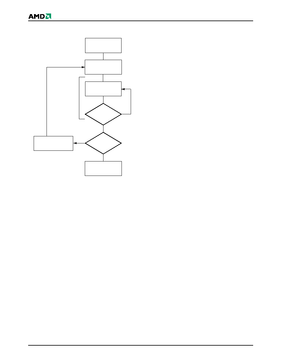
Figure 4.
Program Operation
Chip Erase Command Sequence
Chip erase is a six bus cycle operation. The chip erase
command sequence is initiated by writing two unlock
cycles, followed by a set-up command. Two additional
unlock write cycles are then followed by the chip erase
command, which in turn invokes the Embedded Erase
algorithm. The device does not require the system to
preprogram prior to erase. The Embedded Erase algo-
rithm automatically preprograms and verifies the entire
memory for an all zero data pattern prior to electrical
erase. The system is not required to provide any con-
trols or timings during these operations. Table 13
shows the address and data requirements for the chip
erase command sequence.
When the Embedded Erase algorithm is complete,
that bank returns to the read mode and addresses are
no longer latched. The system can determine the sta-
tus of the erase operation by using DQ7, DQ6, DQ2,
or RY/BY#. Refer to the Write Operation Status sec-
tion for information on these status bits.
Any commands written during the chip erase operation
are ignored. Note that SecSi Sector, autoselect, and
CFI functions are unavailable when a [program/erase]
operation is in progress. However, note that a hard-
ware reset immediately terminates the erase opera-
tion. If that occurs, the chip erase command sequence
should be reinitiated once that bank has returned to
reading array data, to ensure data integrity.
Figure 5 illustrates the algorithm for the erase opera-
tion. Refer to the Erase and Program Operations ta-
bles in the AC Characteristics section for parameters,
and Figure 17 section for timing diagrams.
Sector Erase Command Sequence
Sector erase is a six bus cycle operation. The sector
erase command sequence is initiated by writing two
unlock cycles, followed by a set-up command. Two ad-
ditional unlock cycles are written, and are then fol-
lowed by the address of the sector to be erased, and
the sector erase command.Table 13 shows the ad-
dress and data requirements for the sector erase com-
mand sequence.
The device does not require the system to preprogram
prior to erase. The Embedded Erase algorithm auto-
matically programs and verifies the entire memory for
an all zero data pattern prior to electrical erase. The
system is not required to provide any controls or tim-
ings during these operations.
After the command sequence is written, a sector erase
time-out of 50 s occurs. During the time-out period,
additional sector addresses and sector erase com-
mands may be written. Loading the sector erase buffer
may be done in any sequence, and the number of sec-
tors may be from one sector to all sectors. The time
between these additional cycles must be less than 50
s, otherwise erasure may begin. Any sector erase
a ddre ss a nd command fo llo wing the exce ede d
time-out may or may not be accepted. It is recom-
mended that processor interrupts be disabled during
this time to ensure all commands are accepted. The
interrupts can be re-enabled after the last Sector
Erase command is written. Any command other than
S e c t or E r as e or E r ase S u spe n d du ring th e
time-out period resets that bank to the read mode.
The system must rewrite the command sequence and
any additional addresses and commands. Note that
SecSi Sector, autoselect, and CFI functions are un-
available when a [program/erase] operation is in
progress.
The system can monitor DQ3 to determine if the sec-
tor erase timer has timed out (See the section on DQ3:
Sector Erase Timer). The time-out begins from the ris-
ing edge of the final WE# pulse in the command
sequence.
When the Embedded Erase algorithm is complete, the
bank returns to reading array data and addresses are
no longer latched. Note that while the Embedded
Erase operation is in progress, the system can read
START
Write Program
Command Sequence
Data Poll
from System
Verify Data?
No
Yes
Last Address?
No
Yes
Programming
Completed
Increment Address
Embedded
Program
algorithm
in progress
Note: See Table 13 for program command sequence.
相关PDF资料 |
PDF描述 |
|---|---|
| AM29PDL127H85VKIN | 128 Megabit (8 M x 16-Bit) CMOS 3.0 Volt-only, Page Mode Simultaneous Read/Write Flash Memory with Enhanced VersatileIO Control |
| Am29PDL127H88 | 128 Megabit (8 M x 16-Bit) CMOS 3.0 Volt-only, Page Mode Simultaneous Read/Write Flash Memory with Enhanced VersatileIO Control |
| AM29PDL127H83VKI | 128 Megabit (8 M x 16-Bit) CMOS 3.0 Volt-only, Page Mode Simultaneous Read/Write Flash Memory with Enhanced VersatileIO Control |
| AM29SL800CB-100ED | 512K X 16 FLASH 1.8V PROM, 100 ns, PDSO48 |
| AM29SL800CT150FC | 1M X 8 FLASH 1.8V PROM, 150 ns, PDSO48 |
相关代理商/技术参数 |
参数描述 |
|---|---|
| AM29PDL128G70RPEI | 制造商:Spansion 功能描述:FLASH PARALLEL 3V/3.3V 128MBIT 8MX16/4M X 32 70NS 80FBGA - Trays |
| AM29PDL128G80PEF | 制造商:Spansion 功能描述:SPZAM29PDL128G80PEF 128M FLASH EOL100409 |
| AM29PL141BXA | 制造商:AMD 功能描述:* |
| AM29PL141DC | 制造商:Advanced Micro Devices 功能描述:USER PROGRAMMABLE SPECIAL FUNCTION ASIC, 28 Pin, DIP |
| AM29PL160CB-90SF | 制造商:Advanced Micro Devices 功能描述: |
发布紧急采购,3分钟左右您将得到回复。