- 您现在的位置:买卖IC网 > PDF目录166216 > AM29PDL127H85VKI (Spansion Inc.) 128 Megabit (8 M x 16-Bit) CMOS 3.0 Volt-only, Page Mode Simultaneous Read/Write Flash Memory with Enhanced VersatileIO Control PDF资料下载
参数资料
| 型号: | AM29PDL127H85VKI |
| 厂商: | Spansion Inc. |
| 英文描述: | 128 Megabit (8 M x 16-Bit) CMOS 3.0 Volt-only, Page Mode Simultaneous Read/Write Flash Memory with Enhanced VersatileIO Control |
| 中文描述: | 128兆位(8米× 16位),3.0伏的CMOS只,页面模式同步读/写闪存与增强VersatileIO控制记忆 |
| 文件页数: | 37/68页 |
| 文件大小: | 750K |
| 代理商: | AM29PDL127H85VKI |
第1页第2页第3页第4页第5页第6页第7页第8页第9页第10页第11页第12页第13页第14页第15页第16页第17页第18页第19页第20页第21页第22页第23页第24页第25页第26页第27页第28页第29页第30页第31页第32页第33页第34页第35页第36页当前第37页第38页第39页第40页第41页第42页第43页第44页第45页第46页第47页第48页第49页第50页第51页第52页第53页第54页第55页第56页第57页第58页第59页第60页第61页第62页第63页第64页第65页第66页第67页第68页
40
Am29PDL127H
June 30, 2003
ADV ANCE
I N FO RMAT I O N
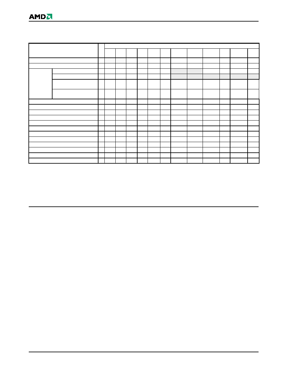
Command Definitions Tables
Legend:
BA = Address of bank switching to autoselect mode, bypass mode, or
erase operation. Determined by A22:A20, see Tables 4 and for more
detail.
PA = Program Address (A22:A0). Addresses latch on falling edge of
WE# or CE# pulse, whichever happens later.
PD = Program Data (DQ15:DQ0) written to location PA. Data latches
on rising edge of WE# or CE# pulse, whichever happens first.
RA = Read Address (A22:A0).
RD = Read Data (DQ15:DQ0) from location RA.
SA = Sector Address (A22:A12) for verifying (in autoselect mode) or
erasing.
WD = Write Data. See “Configuration Register” definition for specific
write data. Data latched on rising edge of WE#.
X = Don’t care
Notes:
1.
See Table 1 for description of bus operations.
2.
All values are in hexadecimal.
3.
Shaded cells in table denote read cycles. All other cycles are
write operations.
4.
During unlock and command cycles, when lower address bits are
555 or 2AAh as shown in table, address bits higher than A11
(except where BA is required) and data bits higher than DQ7 are
don’t cares.
5.
No unlock or command cycles required when bank is reading
array data.
6.
The Reset command is required to return to reading array (or to
erase-suspend-read mode if previously in Erase Suspend) when
bank is in autoselect mode, or if DQ5 goes high (while bank is
providing status information).
7.
Fourth cycle of autoselect command sequence is a read cycle.
System must provide bank address to obtain manufacturer ID or
device ID information. See Autoselect Command Sequence
section for more information.
8.
The data is C0h for factory and customer locked and 80h for
factory locked.
9.
The data is 00h for an unprotected sector group and 01h for a
protected sector group.
10. Device ID must be read across cycles 4, 5, and 6.
11. System may read and program in non-erasing sectors, or enter
autoselect mode, when in Program/Erase Suspend mode.
Program/Erase Suspend command is valid only during a sector
erase operation, and requires bank address.
12. Program/Erase Resume command is valid only during Erase
Suspend mode, and requires bank address.
13. Command is valid when device is ready to read array data or
when device is in autoselect mode.
14. WP#/ACC must be at V
ID during the entire operation of command.
15. Unlock Bypass Entry command is required prior to any Unlock
Bypass operation. Unlock Bypass Reset command is required to
return to the reading array.
Table 13.
Memory Array Command Definitions
Command (Notes)
C
ycl
es
Bus Cycles (Notes 1–4)
Addr Data Addr Data
Addr
Data
Addr
Data
Addr
Data
Addr
Data
Read (5)
1
RA
RD
Reset (6)
1
XXX
F0
Autoselect
Manufacturer ID
4
555
AA
2AA
55
555
90
(BA)X00
01
Device ID (10)
6
555
AA
2AA
55
555
90
(BA)X01
7E
(BA)X0E
20
(BA)X0F
00
SecSi Sector Factory
Protect (8)
4
555
AA
2AA
55
555
90
X03
(see
note 8)
Sector Group Protect Verify
(9)
4
555
AAA
2AA
55
555
90
(SA)X02
XX00/
XX01
Program
4
555
AA
2AA
55
555
A0
PA
PD
Chip Erase
6
555
AA
2AA
55
555
80
555
AA
2AA
55
555
10
Sector Erase
6
555
AA
2AA
55
555
80
555
AA
2AA
55
SA
30
Program/Erase Suspend (11)
1
BA
B0
Program/Erase Resume (12)
1
BA
30
CFI Query (13)
1
55
98
Accelerated Program (15)
2
XX
A0
PA
PD
Unlock Bypass Entry (15)
3
555
AA
2AA
55
555
20
Unlock Bypass Program (15)
2
XX
A0
PA
PD
Unlock Bypass Erase (15)
2
XX
80
XX
10
Unlock Bypass CFI (13, 15)
1
XX
98
Unlock Bypass Reset (15)
2
XXX
90
XXX
00
相关PDF资料 |
PDF描述 |
|---|---|
| AM29PDL127H85VKIN | 128 Megabit (8 M x 16-Bit) CMOS 3.0 Volt-only, Page Mode Simultaneous Read/Write Flash Memory with Enhanced VersatileIO Control |
| Am29PDL127H88 | 128 Megabit (8 M x 16-Bit) CMOS 3.0 Volt-only, Page Mode Simultaneous Read/Write Flash Memory with Enhanced VersatileIO Control |
| AM29PDL127H83VKI | 128 Megabit (8 M x 16-Bit) CMOS 3.0 Volt-only, Page Mode Simultaneous Read/Write Flash Memory with Enhanced VersatileIO Control |
| AM29SL800CB-100ED | 512K X 16 FLASH 1.8V PROM, 100 ns, PDSO48 |
| AM29SL800CT150FC | 1M X 8 FLASH 1.8V PROM, 150 ns, PDSO48 |
相关代理商/技术参数 |
参数描述 |
|---|---|
| AM29PDL128G70RPEI | 制造商:Spansion 功能描述:FLASH PARALLEL 3V/3.3V 128MBIT 8MX16/4M X 32 70NS 80FBGA - Trays |
| AM29PDL128G80PEF | 制造商:Spansion 功能描述:SPZAM29PDL128G80PEF 128M FLASH EOL100409 |
| AM29PL141BXA | 制造商:AMD 功能描述:* |
| AM29PL141DC | 制造商:Advanced Micro Devices 功能描述:USER PROGRAMMABLE SPECIAL FUNCTION ASIC, 28 Pin, DIP |
| AM29PL160CB-90SF | 制造商:Advanced Micro Devices 功能描述: |
发布紧急采购,3分钟左右您将得到回复。