- 您现在的位置:买卖IC网 > PDF目录166216 > Am29PDL127H88 (Spansion Inc.) 128 Megabit (8 M x 16-Bit) CMOS 3.0 Volt-only, Page Mode Simultaneous Read/Write Flash Memory with Enhanced VersatileIO Control PDF资料下载
参数资料
| 型号: | Am29PDL127H88 |
| 厂商: | Spansion Inc. |
| 英文描述: | 128 Megabit (8 M x 16-Bit) CMOS 3.0 Volt-only, Page Mode Simultaneous Read/Write Flash Memory with Enhanced VersatileIO Control |
| 中文描述: | 128兆位(8米× 16位),3.0伏的CMOS只,页面模式同步读/写闪存与增强VersatileIO控制记忆 |
| 文件页数: | 26/68页 |
| 文件大小: | 750K |
| 代理商: | AM29PDL127H88 |
第1页第2页第3页第4页第5页第6页第7页第8页第9页第10页第11页第12页第13页第14页第15页第16页第17页第18页第19页第20页第21页第22页第23页第24页第25页当前第26页第27页第28页第29页第30页第31页第32页第33页第34页第35页第36页第37页第38页第39页第40页第41页第42页第43页第44页第45页第46页第47页第48页第49页第50页第51页第52页第53页第54页第55页第56页第57页第58页第59页第60页第61页第62页第63页第64页第65页第66页第67页第68页
30
Am29PDL127H
June 30, 2003
ADV ANCE
I N FO RMAT I O N
Once the SecSi Sector is locked and verified, the sys-
tem must write the Exit SecSi Sector Region com-
mand sequence to return to reading and writing the
remainder of the array.
The SecSi Sector lock must be used with caution
since, once locked, there is no procedure available for
unlocking the SecSi Sector area and none of the bits
in the SecSi Sector memory space can be modified in
any way.
SecSi Sector Protection Bits
The SecSi Sector Protection Bits prevent program-
ming of the SecSi Sector memory area. Once set, the
SecSi Sector memory area contents are non-modifi-
able.
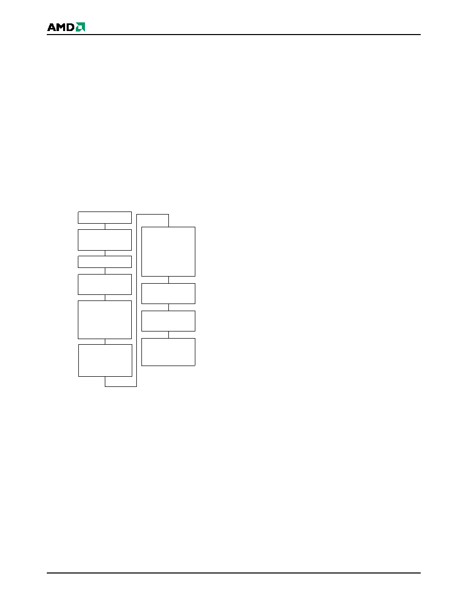
Figure 3.
SecSi Sector Protect Verify
Hardware Data Protection
The command sequence requirement of unlock cycles
for programming or erasing provides data protection
against inadvertent writes. In addition, the following
hardware data protection measures prevent accidental
erasure or programming, which might otherwise be
caused by spurious system level signals during V
CC
power-up and power-down transitions, or from system
noise.
Low VCC Write Inhibit
When V
CC is less than VLKO, the device does not ac-
cept any write cycles. This protects data during V
CC
power-up and power-down. The command register
and all internal program/erase circuits are disabled,
and the device resets to the read mode. Subsequent
writes are ignored until V
CC is greater than VLKO. The
system must provide the proper signals to the control
pins to prevent unintentional writes when V
CC is
greater than V
LKO.
Write Pulse “Glitch” Protection
Noise pulses of less than 3 ns (typical) on OE#, CE#,
or WE# do not initiate a write cycle.
Logical Inhibit
Write cycles are inhibited by holding any one of OE# =
V
IL, CE# = VIH or WE# = VIH. To initiate a write cycle,
CE# and WE# must be a logical zero while OE# is a
logical one.
Power-Up Write Inhibit
If WE# = CE# = V
IL and OE# = VIH during power up,
the device does not accept commands on the rising
edge of WE#. The internal state machine is automati-
cally reset to the read mode on power-up.
COMMON FLASH MEMORY INTERFACE
(CFI)
The Common Flash Interface (CFI) specification out-
lines device and host system software interrogation
handshake, which allows specific vendor-specified
software algorithms to be used for entire families of
devices. Software support can then be device-inde-
pendent, JEDEC ID-independent, and forward- and
backward-compatible for the specified flash device
families. Flash vendors can standardize their existing
interfaces for long-term compatibility.
This device enters the CFI Query mode when the sys-
tem writes the CFI Query command, 98h, to address
55h, any time the device is ready to read array data.
The system can read CFI information at the addresses
the system must write the reset command. The CFI
Query mode is not accessible when the device is exe-
cuting an Embedded Program or embedded Erase al-
gorithm.
The system can also write the CFI query command
when the device is in the autoselect mode. The device
enters the CFI query mode, and the system can read
system must write the reset command to return the de-
vice to reading array data.
For further information, please refer to the CFI Specifi-
cation and CFI Publication 100, available via the
World Wide Web at http://www.amd.com/flash/cfi. Al-
ternatively, contact an AMD representative for copies
of these documents.
Write 60h to
any address
Write 40h to SecSi
Sector address
with A6 = 0,
A1 = 1, A0 = 0
START
RESET# =
VIH or VID
Wait 1
s
Read from SecSi
Sector address
with A6 = 0,
A1 = 1, A0 = 0
If data = 00h,
SecSi Sector is
unprotected.
If data = 01h,
SecSi Sector is
protected.
Remove VIH or VID
from RESET#
Write reset
command
SecSi Sector
Protect Verify
complete
相关PDF资料 |
PDF描述 |
|---|---|
| AM29PDL127H83VKI | 128 Megabit (8 M x 16-Bit) CMOS 3.0 Volt-only, Page Mode Simultaneous Read/Write Flash Memory with Enhanced VersatileIO Control |
| AM29SL800CB-100ED | 512K X 16 FLASH 1.8V PROM, 100 ns, PDSO48 |
| AM29SL800CT150FC | 1M X 8 FLASH 1.8V PROM, 150 ns, PDSO48 |
| AM42BDS640AGBC8IS | Stacked Multi-Chip Package (MCP) Flash Memory and SRAM |
| AM42BDS640AGBC8IT | Stacked Multi-Chip Package (MCP) Flash Memory and SRAM |
相关代理商/技术参数 |
参数描述 |
|---|---|
| AM29PDL128G70RPEI | 制造商:Spansion 功能描述:FLASH PARALLEL 3V/3.3V 128MBIT 8MX16/4M X 32 70NS 80FBGA - Trays |
| AM29PDL128G80PEF | 制造商:Spansion 功能描述:SPZAM29PDL128G80PEF 128M FLASH EOL100409 |
| AM29PL141BXA | 制造商:AMD 功能描述:* |
| AM29PL141DC | 制造商:Advanced Micro Devices 功能描述:USER PROGRAMMABLE SPECIAL FUNCTION ASIC, 28 Pin, DIP |
| AM29PL160CB-90SF | 制造商:Advanced Micro Devices 功能描述: |
发布紧急采购,3分钟左右您将得到回复。