- 您现在的位置:买卖IC网 > PDF目录166216 > Am29PDL127H88 (Spansion Inc.) 128 Megabit (8 M x 16-Bit) CMOS 3.0 Volt-only, Page Mode Simultaneous Read/Write Flash Memory with Enhanced VersatileIO Control PDF资料下载
参数资料
| 型号: | Am29PDL127H88 |
| 厂商: | Spansion Inc. |
| 英文描述: | 128 Megabit (8 M x 16-Bit) CMOS 3.0 Volt-only, Page Mode Simultaneous Read/Write Flash Memory with Enhanced VersatileIO Control |
| 中文描述: | 128兆位(8米× 16位),3.0伏的CMOS只,页面模式同步读/写闪存与增强VersatileIO控制记忆 |
| 文件页数: | 39/68页 |
| 文件大小: | 750K |
| 代理商: | AM29PDL127H88 |
第1页第2页第3页第4页第5页第6页第7页第8页第9页第10页第11页第12页第13页第14页第15页第16页第17页第18页第19页第20页第21页第22页第23页第24页第25页第26页第27页第28页第29页第30页第31页第32页第33页第34页第35页第36页第37页第38页当前第39页第40页第41页第42页第43页第44页第45页第46页第47页第48页第49页第50页第51页第52页第53页第54页第55页第56页第57页第58页第59页第60页第61页第62页第63页第64页第65页第66页第67页第68页
42
Am29PDL127H
June 30, 2003
ADV ANCE
I N FO RMAT I O N
WRITE OPERATION STATUS
The device provides several bits to determine the status of
a program or erase operation: DQ2, DQ3, DQ5, DQ6, and
DQ7. Table 15 and the following subsections describe the
function of these bits. DQ7 and DQ6 each offer a method
for determining whether a program or erase operation is
complete or in progress. The device also provides a hard-
ware-based output signal, RY/BY#, to determine whether
an Embedded Program or Erase operation is in progress or
has been completed.
DQ7: Data# Polling
The Data# Polling bit, DQ7, indicates to the host system
whether an Embedded Program or Erase algorithm is in
progress or completed, or whether a bank is in Erase Sus-
pend. Data# Polling is valid after the rising edge of the final
WE# pulse in the command sequence.
During the Embedded Program algorithm, the device out-
puts on DQ7 the complement of the datum programmed to
DQ7. This DQ7 status also applies to programming during
Erase Suspend. When the Embedded Program algorithm is
complete, the device outputs the datum programmed to
DQ7. The system must provide the program address to
read valid status information on DQ7. If a program address
falls within a protected sector, Data# Polling on DQ7 is ac-
tive for approximately 1 s, then that bank returns to the
read mode.
During the Embedded Erase algorithm, Data# Polling
produces a “0” on DQ7. When the Embedded Erase
algorithm is complete, or if the bank enters the Erase
Suspend mode, Data# Polling produces a “1” on DQ7.
The system must provide an address within any of the
sectors selected for erasure to read valid status infor-
mation on DQ7.
After an erase command sequence is written, if all
sectors selected for erasing are protected, Data# Poll-
ing on DQ7 is active for approximately 400 s, then
the bank returns to the read mode. If not all selected
sectors are protected, the Embedded Erase algorithm
erases the unprotected sectors, and ignores the se-
lected sectors that are protected. However, if the sys-
tem reads DQ7 at an address within a protected
sector, the status may not be valid.
When the system detects DQ7 has changed from the
complement to true data, it can read valid data at
DQ15–DQ0 on the following read cycles. Just prior to
the completion of an Embedded Program or Erase op-
eration, DQ7 may change asynchronously with
DQ15–DQ0 while Output Enable (OE#) is asserted
low. That is, the device may change from providing
status information to valid data on DQ7. Depending on
when the system samples the DQ7 output, it may read
the status or valid data. Even if the device has com-
pleted the program or erase operation and DQ7 has
valid data, the data outputs on DQ15–DQ0 may be still
invalid. Valid data on DQ15–DQ0 will appear on suc-
cessive read cycles.
Table 15 shows the outputs for Data# Polling on DQ7.
in the AC Characteristic section shows the Data# Poll-
ing timing diagram.
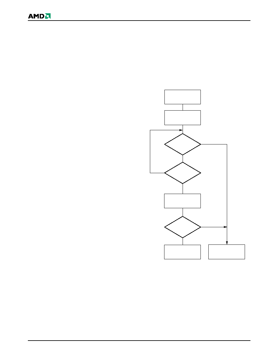
Figure 6.
Data# Polling Algorithm
DQ7 = Data?
Yes
No
DQ5 = 1?
No
Yes
FAIL
PASS
Read DQ7–DQ0
Addr = VA
Read DQ7–DQ0
Addr = VA
DQ7 = Data?
START
Notes:
1. VA = Valid address for programming. During a sector
erase operation, a valid address is any sector address
within the sector being erased. During chip erase, a
valid address is any non-protected sector address.
2. DQ7 should be rechecked even if DQ5 = “1” because
DQ7 may change simultaneously with DQ5.
相关PDF资料 |
PDF描述 |
|---|---|
| AM29PDL127H83VKI | 128 Megabit (8 M x 16-Bit) CMOS 3.0 Volt-only, Page Mode Simultaneous Read/Write Flash Memory with Enhanced VersatileIO Control |
| AM29SL800CB-100ED | 512K X 16 FLASH 1.8V PROM, 100 ns, PDSO48 |
| AM29SL800CT150FC | 1M X 8 FLASH 1.8V PROM, 150 ns, PDSO48 |
| AM42BDS640AGBC8IS | Stacked Multi-Chip Package (MCP) Flash Memory and SRAM |
| AM42BDS640AGBC8IT | Stacked Multi-Chip Package (MCP) Flash Memory and SRAM |
相关代理商/技术参数 |
参数描述 |
|---|---|
| AM29PDL128G70RPEI | 制造商:Spansion 功能描述:FLASH PARALLEL 3V/3.3V 128MBIT 8MX16/4M X 32 70NS 80FBGA - Trays |
| AM29PDL128G80PEF | 制造商:Spansion 功能描述:SPZAM29PDL128G80PEF 128M FLASH EOL100409 |
| AM29PL141BXA | 制造商:AMD 功能描述:* |
| AM29PL141DC | 制造商:Advanced Micro Devices 功能描述:USER PROGRAMMABLE SPECIAL FUNCTION ASIC, 28 Pin, DIP |
| AM29PL160CB-90SF | 制造商:Advanced Micro Devices 功能描述: |
发布紧急采购,3分钟左右您将得到回复。