- 您现在的位置:买卖IC网 > PDF目录378403 > AN1406 (ON SEMICONDUCTOR) DESIGNING WITH PECL (ECL AT + 5.0) PDF资料下载
参数资料
| 型号: | AN1406 |
| 厂商: | ON SEMICONDUCTOR |
| 英文描述: | DESIGNING WITH PECL (ECL AT + 5.0) |
| 中文描述: | 具有PECL设计(ECL在5.0) |
| 文件页数: | 3/8页 |
| 文件大小: | 117K |
| 代理商: | AN1406 |
AN1406/D
http://onsemi.com
3
reduced while maintaining acceptable manufacturing
yields.
What does this mean to the CMOS/TTL designer It
means that CMOS/TTL designers can build their clock
generation card and backplane clock distribution using
ECL. Designers will not only realize the benefits of driving
long lines with ECL but will also be able to realize clock
distribution networks with skew specs unheard of in the
CMOS/TTL world. Many specialized functions for clock
distribution are available from Motorola (MC10/100E111,
MC10/100E211, MC10/100EL11). Care must be taken that
all of the skew gained using ECL for clock distribution is not
lost in the process of translating into CMOS/TTL levels. To
alleviate this problem the MC10/100H646 can be used to
translate and fanout a differential ECL input signal into TTL
levels. In this way all of the fanout on the backplane can be
done in ECL while the fanout on each card can be done in the
CMOS/TTL levels necessary to drive the logic.
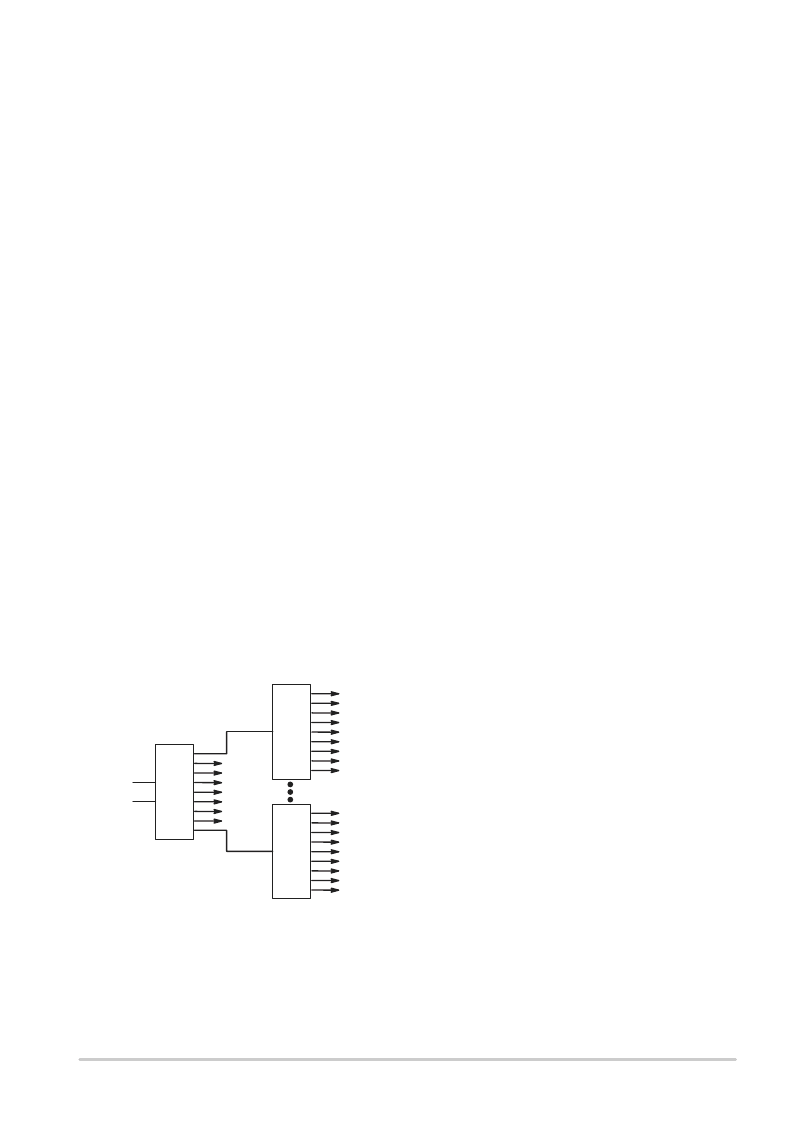
Figure 2 illustrates the use of specialized fanout buffers to
design a CMOS/TTL clock distribution network with
minimal skew. With 50ps output–to–output skew of the
MC10/100E111 and 1ns part–to–part skew available on the
MC10/100H646 or MC10/100H641, a total of 72 or 81 TTL
clocks, respectively, can be generated with a worst case
skew between all outputs of only 1.05ns. A similar
distribution tree using octal CMOS or TTL buffers would
result in worst case skews of more than 6ns. This 5ns
improvement in skew equates to about 50% of the up/down
time of a 50MHz clock cycle. It is not difficult to imagine
situations where an extra 50% of time to perform necessary
operations would be either beneficial or even a life saver. For
more information about using ECL for clock distribution,
refer to application note AN1405/D – ECL Clock
Distribution Techniques.
Figure 2. Low Skew Clock Fanout Tree
Differential
ECL Input
1 of 9
H641
Part–Part
Skew = 1ns
TTL
Outputs
9 of 9
H641
TTL
Outputs
E111
Output–Output
Skew = 50ps
D
PECL versus ECL
Nobody will argue that the benefits presented thus far are
not attractive, however the argument will be made that the
benefits are not enough to justify the requirements of
including ECL devices in a predominantly CMOS/TTL
design. After all the inclusion of ECL requires two
additional negative voltage supplies; VEE and the
terminating voltage VTT. Fortunately this is where the
advantages of PECL come into play. By using ECL devices
on a positive five volt CMOS/TTL power supply and using
specialized termination techniques ECL logic can be
incorporated into CMOS/TTL designs without the need for
additional power supplies. What about power dissipation
you ask, although it is true that in a DC state ECL will
typically dissipate more power than a CMOS/TTL
counterpart, in applications which operate continually at
frequency, i.e.. clock distribution, the disparity between
ECL and CMOS/TTL power dissipation is reduced. The
power dissipation of an ECL device remains constant with
frequency while the power of a CMOS/TTL device will
increase with frequency. As frequencies approach 50MHz
the difference between the power dissipation of a CMOS or
TTL gate and an ECL gate will be minimal. 50MHz clock
speeds are becoming fairly common in CMOS/TTL based
designs as today’s high performance MPUs are fast
approaching these speeds. In addition, because ECL output
swings are significantly less than those of CMOS and TTL
the power dissipated in the load will be significantly less
under continuous AC conditions.
It is clear that PECL can be a powerful design tool for
CMOS/TTL designers, but where can one get these PECL
devices. Perhaps the most confusing aspect of PECL is the
misconception that a PECL device is a special adaptation of
an ECL device. In reality
every
ECL device is also a PECL
device; there is nothing magical about the negative voltage
supply used for ECL devices. The only real requirement of
the power supplies is that the potential difference described
in the device data sheets appears across the upper and lower
power supply rails (VCC and VEE respectively). A potential
stumbling block arises in the specified VEE levels for the
various ECL families. The 10H and 100K families specify
parametric values for potential differences between VCC and
VEE of 4.94V to 5.46V and 4.2V to 4.8V respectively; this
poses a problem for the CMOS/TTL designer who works
with a typical VCC of 5.0V
±
5%. However, because both of
these ECL standards are voltage compensated both families
will operate perfectly fine and meet all of the performance
specifications when operated on standard CMOS/TTL
power supplies. In fact, Motorola is extending the VEE
specification ranges of many of their ECL families to be
compatible with standard CMOS/TTL power supplies.
Unfortunately earlier ECL families such as MECL 10K
are not voltage compensated and therefore any reduction in
the potential difference between the two supplies will result
in an increase in the VOL level, and thus a decreased noise
margin. For the typical CMOS/TTL power supplies a 10K
device will experience an
≈
50mV increase in the VOL level.
Designers should analyze whether this loss of noise margin
could jeopardize their designs before implementing PECL
formatted 10K using 5.0V
±
5% power supplies.
相关PDF资料 |
PDF描述 |
|---|---|
| AN1504 | Metastability and the ECLinPS Family |
| AN1504D | Metastability and the ECLinPS Family |
| AN1568 | Interfacing Between LVDS and ECL |
| AN1568D | Interfacing Between LVDS and ECL |
| AN1593 | LOW COST 1.0 A CURRENT SOURCE FOR BATTERY CHARGERS |
相关代理商/技术参数 |
参数描述 |
|---|---|
| AN1406/D | 制造商:ONSEMI 制造商全称:ON Semiconductor 功能描述:DESIGNING WITH PECL (ECL AT + 5.0) |
| AN1406D | 制造商:ONSEMI 制造商全称:ON Semiconductor 功能描述:3.3V / 5V ECL 2-Input Differential XOR/XNOR |
| AN14-17A | 制造商:AN# - MILITARY 功能描述: |
| AN1431 | 制造商:PANASONIC 制造商全称:Panasonic Semiconductor 功能描述:Surface-mount Adjustable Output Shunt Regulator |
| AN1431M | 功能描述:IC VREF SHUNT ADJ TO-243 RoHS:是 类别:集成电路 (IC) >> PMIC - 电压基准 系列:- 产品培训模块:Voltage Reference Basics 标准包装:100 系列:- 基准类型:旁路,精度 输出电压:4.096V 容差:±0.075% 温度系数:50ppm/°C 输入电压:- 通道数:1 电流 - 阴极:1µA 电流 - 静态:- 电流 - 输出:10mA 工作温度:0°C ~ 70°C 安装类型:表面贴装 封装/外壳:8-SOIC(0.154",3.90mm 宽) 供应商设备封装:8-SOIC 包装:管件 |
发布紧急采购,3分钟左右您将得到回复。