- 您现在的位置:买卖IC网 > PDF目录295111 > AT40K40LV-3EQC (ATMEL CORP) FPGA, 2304 CLBS, 40000 GATES, PQFP240 PDF资料下载
参数资料
| 型号: | AT40K40LV-3EQC |
| 厂商: | ATMEL CORP |
| 元件分类: | FPGA |
| 英文描述: | FPGA, 2304 CLBS, 40000 GATES, PQFP240 |
| 封装: | PLASTIC, QFP-240 |
| 文件页数: | 4/67页 |
| 文件大小: | 1589K |
| 代理商: | AT40K40LV-3EQC |
第1页第2页第3页当前第4页第5页第6页第7页第8页第9页第10页第11页第12页第13页第14页第15页第16页第17页第18页第19页第20页第21页第22页第23页第24页第25页第26页第27页第28页第29页第30页第31页第32页第33页第34页第35页第36页第37页第38页第39页第40页第41页第42页第43页第44页第45页第46页第47页第48页第49页第50页第51页第52页第53页第54页第55页第56页第57页第58页第59页第60页第61页第62页第63页第64页第65页第66页第67页
12
AT40K/AT40KLV Series FPGA
0896C–FPGA–04/02
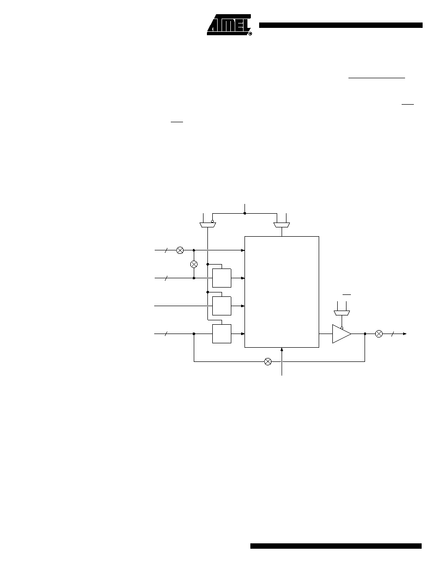
Reading and writing of the 10 ns 32 x 4 dual-port FreeRAM are independent of each
other. Reading the 32 x 4 dual-port RAM is completely asynchronous. Latches are
transparent; when Load is logic 1, data flows through; when Load is logic 0, data is
latched. These latches are used to synchronize Write Address, Write Enable Not,and
Din signals for a synchronous RAM. Each bit in the 32 x 4 dual-port RAM is also a trans-
parent latch. The front-end latch and the memory latch together form an edge-triggered
flip flop. When a nibble (bit = 7) is (Write) addressed and LOAD is logic 1 and WE is
logic 0, data flows through the bit. When a nibble is not (Write) addressed or LOAD is
logic 0 or WE is logic 1, data is latched in the nibble. The two CLOCK muxes are con-
trolled together; they both select CLOCK (for a synchronous RAM) or they both select
“1” (for an asynchronous RAM). CLOCK is obtained from the clock for the sector-column
immediately to the left and immediately above the RAM block. Writing any value to the
RAM clear byte during configuration clears the RAM (see the “
AT40K Configuration
Series” application note at www.atmel.com).
Figure 8. RAM Logic
Figure 9 on page 13 shows an example of a RAM macro constructed using the
AT40K/AT40KLV’s FreeRAM cells. The macro shown is a 128 x 8 dual-ported asyn-
chronous RAM. Note the very small amount of external logic required to complete the
address decoding for the macro. Most of the logic cells (core cells) in the sectors occu-
pied by the RAM will be unused: they can be used for other logic in the design. This
logic can be automatically generated using the macro generators.
Write Address
Din
Dout
Read Address
“1”
Write Enable NOT
RAM-Clear Byte
Dout
01
0
1
“1”
CLOCK
Load
5
Ain
Aout
WEN
Din
Load
Latch
Load
Latch
Load
Latch
Clear
32 x 4
Dual-port
RAM
OE
4
5
相关PDF资料 |
PDF描述 |
|---|---|
| AT40K40LV-3FQC | FPGA, 2304 CLBS, 40000 GATES, PQFP304 |
| AT40KEL040KW1SB | FPGA, 2304 CLBS, 50000 GATES, PQFP160 |
| AT40KEL040KZ1SB | FPGA, 2304 CLBS, 50000 GATES, PQFP256 |
| AT89C2051-12SCT/R | 8-BIT, FLASH, 12 MHz, MICROCONTROLLER, PDSO20 |
| AT89C51-24JCT/R | 8-BIT, FLASH, 24 MHz, MICROCONTROLLER, PQCC44 |
相关代理商/技术参数 |
参数描述 |
|---|---|
| AT40K40LV-3EQI | 功能描述:IC FPGA 3.3V 2304 CELL 240PQFP RoHS:否 类别:集成电路 (IC) >> 嵌入式 - FPGA(现场可编程门阵列) 系列:AT40K/KLV 产品变化通告:XC4000(E,L) Discontinuation 01/April/2002 标准包装:24 系列:XC4000E/X LAB/CLB数:100 逻辑元件/单元数:238 RAM 位总计:3200 输入/输出数:80 门数:3000 电源电压:4.5 V ~ 5.5 V 安装类型:表面贴装 工作温度:-40°C ~ 100°C 封装/外壳:120-BCBGA 供应商设备封装:120-CPGA(34.55x34.55) |
| AT40K40LV-3FQC | 制造商:Atmel Corporation 功能描述:FPGA 50K GATES 2304 CELLS COMM 0.6UM 3.3V 304PQFP - Trays |
| AT40K40LV-3FQI | 功能描述:IC FPGA 3.3V 2304 CELL 304PQFP RoHS:否 类别:集成电路 (IC) >> 嵌入式 - FPGA(现场可编程门阵列) 系列:AT40K/KLV 产品变化通告:XC4000(E,L) Discontinuation 01/April/2002 标准包装:24 系列:XC4000E/X LAB/CLB数:100 逻辑元件/单元数:238 RAM 位总计:3200 输入/输出数:80 门数:3000 电源电压:4.5 V ~ 5.5 V 安装类型:表面贴装 工作温度:-40°C ~ 100°C 封装/外壳:120-BCBGA 供应商设备封装:120-CPGA(34.55x34.55) |
| AT40KAL | 制造商:未知厂家 制造商全称:未知厂家 功能描述:AT40KAL Preliminary [Updated 6/03. 38 Pages] |
| AT40KAL040KW1M | 制造商:ATMEL 制造商全称:ATMEL Corporation 功能描述:Military Reprogrammable FPGAs with FreeRAM |
发布紧急采购,3分钟左右您将得到回复。