- 您现在的位置:买卖IC网 > PDF目录295111 > AT40K40LV-3EQC (ATMEL CORP) FPGA, 2304 CLBS, 40000 GATES, PQFP240 PDF资料下载
参数资料
| 型号: | AT40K40LV-3EQC |
| 厂商: | ATMEL CORP |
| 元件分类: | FPGA |
| 英文描述: | FPGA, 2304 CLBS, 40000 GATES, PQFP240 |
| 封装: | PLASTIC, QFP-240 |
| 文件页数: | 66/67页 |
| 文件大小: | 1589K |
| 代理商: | AT40K40LV-3EQC |
第1页第2页第3页第4页第5页第6页第7页第8页第9页第10页第11页第12页第13页第14页第15页第16页第17页第18页第19页第20页第21页第22页第23页第24页第25页第26页第27页第28页第29页第30页第31页第32页第33页第34页第35页第36页第37页第38页第39页第40页第41页第42页第43页第44页第45页第46页第47页第48页第49页第50页第51页第52页第53页第54页第55页第56页第57页第58页第59页第60页第61页第62页第63页第64页第65页当前第66页第67页
8
AT40K/AT40KLV Series FPGA
0896C–FPGA–04/02
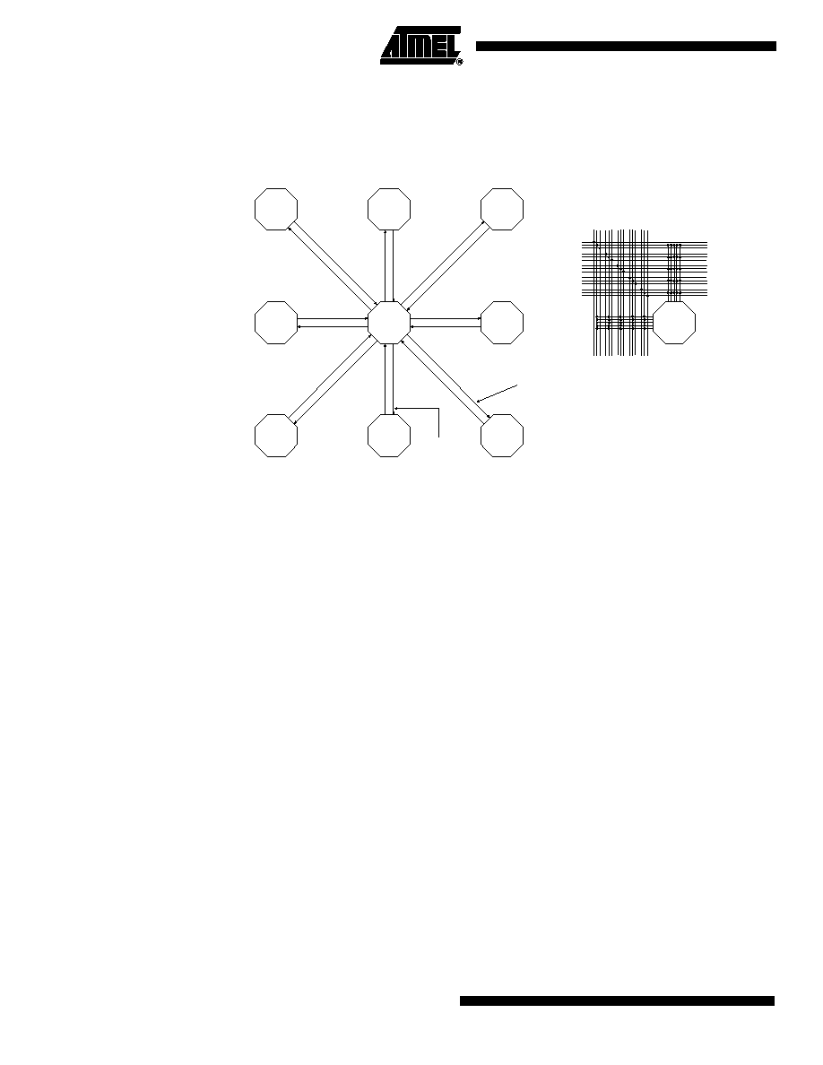
Cell Connections
Figure 4(a) depicts direct connections between a cell and its eight nearest neighbors.
Figure 4(b) shows the connections between a cell and five horizontal local buses (1 per
busing plane) and five vertical local buses (1 per busing plane).
Figure 4. Cell Connections
The Cell
Figure 5 depicts the AT40K/AT40KLV cell. Configuration bits for separate muxes and
pass gates are independent. All permutations of programmable muxes and pass gates
are legal. Vn (V1 -V5) is connected to the vertical local bus in plane n. Hn (H1 -H5)is
connected to the horizontal local bus in plane
n. A local/local turn in plane n is achieved
by turning on the two pass gates connected to Vn and Hn. Pass gates are opened to let
signals into the cell from a local bus or to drive a signal out onto a local bus. Signals
coming into the logic cell on one local bus plane can be switched onto another plane by
opening two of the pass gates. This allows bus signals to switch planes to achieve
greater route ability. Up to five simultaneous local/local turns are possible.
The AT40K/AT40KLV FPGA core cell is a highly configurable logic block based around
two 3-input LUTs (8 x 1 ROM), which can be combined to produce one 4-input LUT.
This means that any core cell can implement two functions of 3 inputs or one function of
4 inputs. There is a Set/Reset D flip-flop in every cell, the output of which may be tri-
stated and fed back internally within the core cell. There is also a 2-to-1 multiplexer in
every cell, and an upstream AND gate in the “front end” of the cell. This AND gate is an
important feature in the implementation of efficient array multipliers.
With this functionality in each core cell, the core cell can be configured in several
“modes”. The core cell flexibility makes the AT40K/AT40KLV architecture well suited to
most digital design application areas, see Figure 6.
CELL
(a) Cell-to-cell Connections
(b) Cell-to-bus Connections
W
X
Y
Z
L
WXYZL
Orthogonal
Direct Connect
Diagonal
Direct Connect
Horizontal
Busing Plane
Vertical
Busing Plane
Plane 5
Plane 4
Plane 3
Plane 2
Plane 1
Plane
5
Plane
4
Plane
3
Plane
2
Plane
1
CELL
相关PDF资料 |
PDF描述 |
|---|---|
| AT40K40LV-3FQC | FPGA, 2304 CLBS, 40000 GATES, PQFP304 |
| AT40KEL040KW1SB | FPGA, 2304 CLBS, 50000 GATES, PQFP160 |
| AT40KEL040KZ1SB | FPGA, 2304 CLBS, 50000 GATES, PQFP256 |
| AT89C2051-12SCT/R | 8-BIT, FLASH, 12 MHz, MICROCONTROLLER, PDSO20 |
| AT89C51-24JCT/R | 8-BIT, FLASH, 24 MHz, MICROCONTROLLER, PQCC44 |
相关代理商/技术参数 |
参数描述 |
|---|---|
| AT40K40LV-3EQI | 功能描述:IC FPGA 3.3V 2304 CELL 240PQFP RoHS:否 类别:集成电路 (IC) >> 嵌入式 - FPGA(现场可编程门阵列) 系列:AT40K/KLV 产品变化通告:XC4000(E,L) Discontinuation 01/April/2002 标准包装:24 系列:XC4000E/X LAB/CLB数:100 逻辑元件/单元数:238 RAM 位总计:3200 输入/输出数:80 门数:3000 电源电压:4.5 V ~ 5.5 V 安装类型:表面贴装 工作温度:-40°C ~ 100°C 封装/外壳:120-BCBGA 供应商设备封装:120-CPGA(34.55x34.55) |
| AT40K40LV-3FQC | 制造商:Atmel Corporation 功能描述:FPGA 50K GATES 2304 CELLS COMM 0.6UM 3.3V 304PQFP - Trays |
| AT40K40LV-3FQI | 功能描述:IC FPGA 3.3V 2304 CELL 304PQFP RoHS:否 类别:集成电路 (IC) >> 嵌入式 - FPGA(现场可编程门阵列) 系列:AT40K/KLV 产品变化通告:XC4000(E,L) Discontinuation 01/April/2002 标准包装:24 系列:XC4000E/X LAB/CLB数:100 逻辑元件/单元数:238 RAM 位总计:3200 输入/输出数:80 门数:3000 电源电压:4.5 V ~ 5.5 V 安装类型:表面贴装 工作温度:-40°C ~ 100°C 封装/外壳:120-BCBGA 供应商设备封装:120-CPGA(34.55x34.55) |
| AT40KAL | 制造商:未知厂家 制造商全称:未知厂家 功能描述:AT40KAL Preliminary [Updated 6/03. 38 Pages] |
| AT40KAL040KW1M | 制造商:ATMEL 制造商全称:ATMEL Corporation 功能描述:Military Reprogrammable FPGAs with FreeRAM |
发布紧急采购,3分钟左右您将得到回复。