- 您现在的位置:买卖IC网 > PDF目录295111 > AT40K40LV-3EQC (ATMEL CORP) FPGA, 2304 CLBS, 40000 GATES, PQFP240 PDF资料下载
参数资料
| 型号: | AT40K40LV-3EQC |
| 厂商: | ATMEL CORP |
| 元件分类: | FPGA |
| 英文描述: | FPGA, 2304 CLBS, 40000 GATES, PQFP240 |
| 封装: | PLASTIC, QFP-240 |
| 文件页数: | 56/67页 |
| 文件大小: | 1589K |
| 代理商: | AT40K40LV-3EQC |
第1页第2页第3页第4页第5页第6页第7页第8页第9页第10页第11页第12页第13页第14页第15页第16页第17页第18页第19页第20页第21页第22页第23页第24页第25页第26页第27页第28页第29页第30页第31页第32页第33页第34页第35页第36页第37页第38页第39页第40页第41页第42页第43页第44页第45页第46页第47页第48页第49页第50页第51页第52页第53页第54页第55页当前第56页第57页第58页第59页第60页第61页第62页第63页第64页第65页第66页第67页
6
AT40K/AT40KLV Series FPGA
0896C–FPGA–04/02
The Busing Network
Figure 3 on page 7 depicts one of five identical busing planes. Each plane has three bus
resources: a local-bus resource (the middle bus) and two express-bus (both sides)
resources. Bus resources are connected via repeaters. Each repeater has connections
to two adjacent local-bus segments and two express-bus segments. Each local-bus
segment spans four cells and connects to consecutive repeaters. Each express-bus
segment spans eight cells and “leapfrogs” or bypasses a repeater. Repeaters regener-
ate signals and can connect any bus to any other bus (all pathways are legal) on the
same plane. Although not shown, a local bus can bypass a repeater via a programma-
ble pass gate allowing long on-chip tri-state buses to be created. Local/Local turns are
implemented through pass gates in the cell-bus interface. Express/Express turns are
implemented through separate pass gates distributed throughout the array.
Some of the bus resources on the AT40K/AT40KLV are used as a dual-function
resources. Table 2 shows which buses are used in a dual-function mode and which bus
plane is used. The AT40K/AT40KLV software tools are designed to accommodate dual-
function buses in an efficient manner.
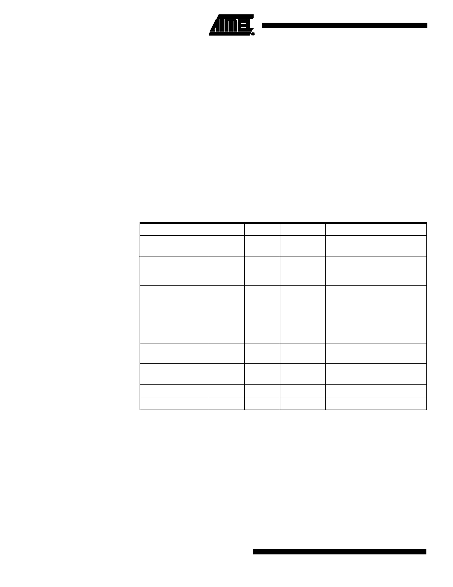
Table 2. Dual-function Buses
Function
Type
Plane(s)
Direction
Comments
Cell Output Enable
Local
5
Horizontal
and Vertical
RAM Output Enable
Express
2
Vertical
Bus full length at array edge
Bus in first column to left of
RAM block
RAM Write Enable
Express
1
Vertical
Bus full length at array edge
Bus in first column to left of
RAM block
RAM Address
Express
1 - 5
Vertical
Buses full length at array edge
Buses in second column to left
of RAM block
RAM Data In
Local
1
Horizontal
Data In connects to local
bus plane 1
RAM Data Out
Local
2
Horizontal
Data out connects to local
bus plane 2
Clocking
Express
4
Vertical
Bus half length at array edge
Set/Reset
Express
5
Vertical
Bus half length at array edge
相关PDF资料 |
PDF描述 |
|---|---|
| AT40K40LV-3FQC | FPGA, 2304 CLBS, 40000 GATES, PQFP304 |
| AT40KEL040KW1SB | FPGA, 2304 CLBS, 50000 GATES, PQFP160 |
| AT40KEL040KZ1SB | FPGA, 2304 CLBS, 50000 GATES, PQFP256 |
| AT89C2051-12SCT/R | 8-BIT, FLASH, 12 MHz, MICROCONTROLLER, PDSO20 |
| AT89C51-24JCT/R | 8-BIT, FLASH, 24 MHz, MICROCONTROLLER, PQCC44 |
相关代理商/技术参数 |
参数描述 |
|---|---|
| AT40K40LV-3EQI | 功能描述:IC FPGA 3.3V 2304 CELL 240PQFP RoHS:否 类别:集成电路 (IC) >> 嵌入式 - FPGA(现场可编程门阵列) 系列:AT40K/KLV 产品变化通告:XC4000(E,L) Discontinuation 01/April/2002 标准包装:24 系列:XC4000E/X LAB/CLB数:100 逻辑元件/单元数:238 RAM 位总计:3200 输入/输出数:80 门数:3000 电源电压:4.5 V ~ 5.5 V 安装类型:表面贴装 工作温度:-40°C ~ 100°C 封装/外壳:120-BCBGA 供应商设备封装:120-CPGA(34.55x34.55) |
| AT40K40LV-3FQC | 制造商:Atmel Corporation 功能描述:FPGA 50K GATES 2304 CELLS COMM 0.6UM 3.3V 304PQFP - Trays |
| AT40K40LV-3FQI | 功能描述:IC FPGA 3.3V 2304 CELL 304PQFP RoHS:否 类别:集成电路 (IC) >> 嵌入式 - FPGA(现场可编程门阵列) 系列:AT40K/KLV 产品变化通告:XC4000(E,L) Discontinuation 01/April/2002 标准包装:24 系列:XC4000E/X LAB/CLB数:100 逻辑元件/单元数:238 RAM 位总计:3200 输入/输出数:80 门数:3000 电源电压:4.5 V ~ 5.5 V 安装类型:表面贴装 工作温度:-40°C ~ 100°C 封装/外壳:120-BCBGA 供应商设备封装:120-CPGA(34.55x34.55) |
| AT40KAL | 制造商:未知厂家 制造商全称:未知厂家 功能描述:AT40KAL Preliminary [Updated 6/03. 38 Pages] |
| AT40KAL040KW1M | 制造商:ATMEL 制造商全称:ATMEL Corporation 功能描述:Military Reprogrammable FPGAs with FreeRAM |
发布紧急采购,3分钟左右您将得到回复。